Process and apparatus for treating a substrate
- Summary
- Abstract
- Description
- Claims
- Application Information
AI Technical Summary
Benefits of technology
Problems solved by technology
Method used
Image
Examples
first embodiment
In the present invention, etching process to which the present invention is applied will be explained. An object to be etched is a silicon oxide film deposited on a silicon substrate, and an opening corresponding to a contact hole to be made in the course of a semiconductor production process will be made according to a process of the present invention. A main object of this process is to ensure a selection ratio of etching SiO.sub.2 while maintaining a sufficient etching speed. In order to attain this object, a gas mixture of CF.sub.3 I, CF.sub.2 I.sub.2 and CFI.sub.3, that are substituted CF.sub.4 whose halogen elements are partially substituted by iodine, was used for a treating gas for carrying out the present invention.
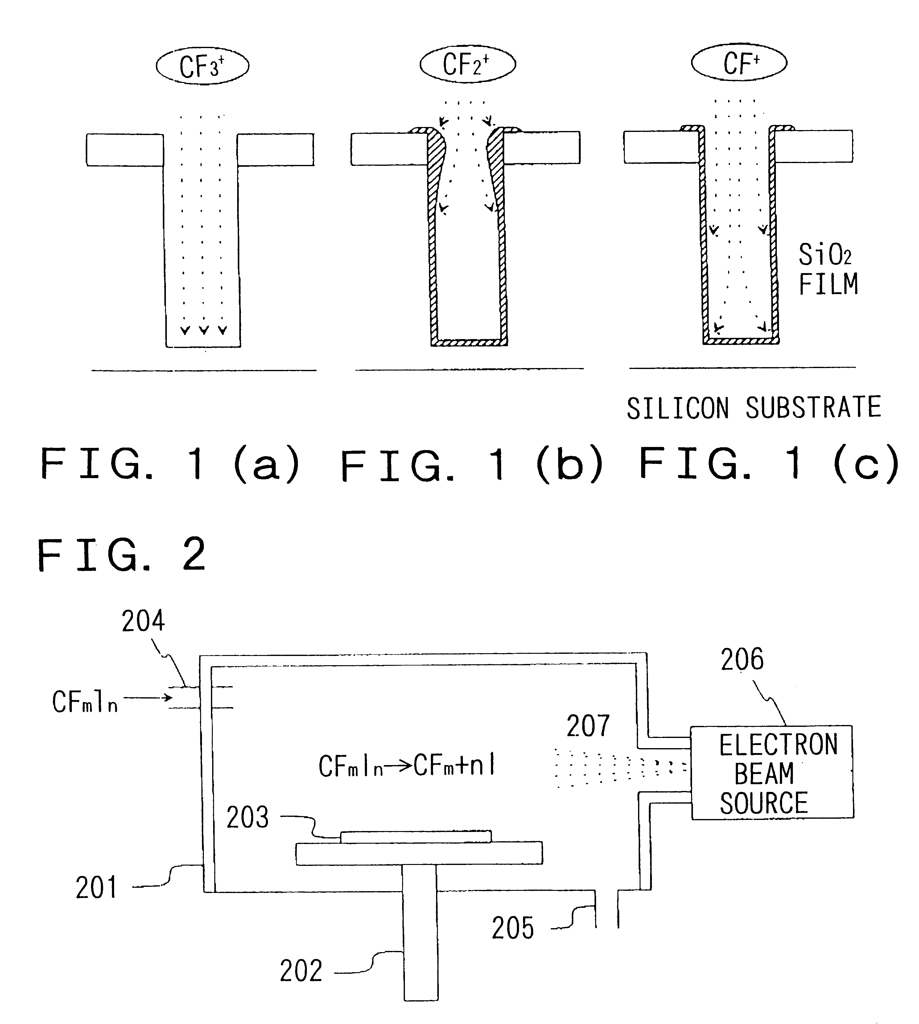
FIG. 1 is a schematic view showing a role of each ion or radical in case of etching SiO.sub.2 / Si (a SiO.sub.2 film deposited on a Si substrate) by using a CF.sub.4 series of gas. Among the ions and radicals resulting from the dissociation of CF.sub.4, CF.sub.3.s...
example 1
Example 1 of the present invention relates to a case of using an energy-controlled electron beam for an excitation means for producing radicals from the above mixed gas.
FIG. 2 shows a rough view of an etching apparatus used in carrying out this example. The etching apparatus has a substrate holder 202 in a vacuum chamber 201 made of stainless steel and a substrate 203 to be treated held on the substrate holder 202. A treating gas is introduced into the vacuum chamber 201 through an inlet 204 for charging the treating gas. The gas in the vacuum chamber is discharged through an outlet 205 by vacuum discharging with a discharge pump which is not shown in any figure of the accompanying drawings. On the side of the vacuum chamber 201 an electron beam source 206 is installed. An electron beam 207 illustrated by a broken line is irradiated from this electron beam source 206 into the vacuum chamber 201. The treating gas is dissociated by the action of the electron beam 207 to produce radica...
example 2
In this example, a case of etching a substrate by radical and / or ion resulting from exciting a gas mixture of CF.sub.3 I, CF.sub.2 I.sub.2 and CFI.sub.3 by means of plasma is referred. Used plasma was UHF plasma produced by the application of high frequency of VHF to UHF band (about 100 to 1,000 MHz).
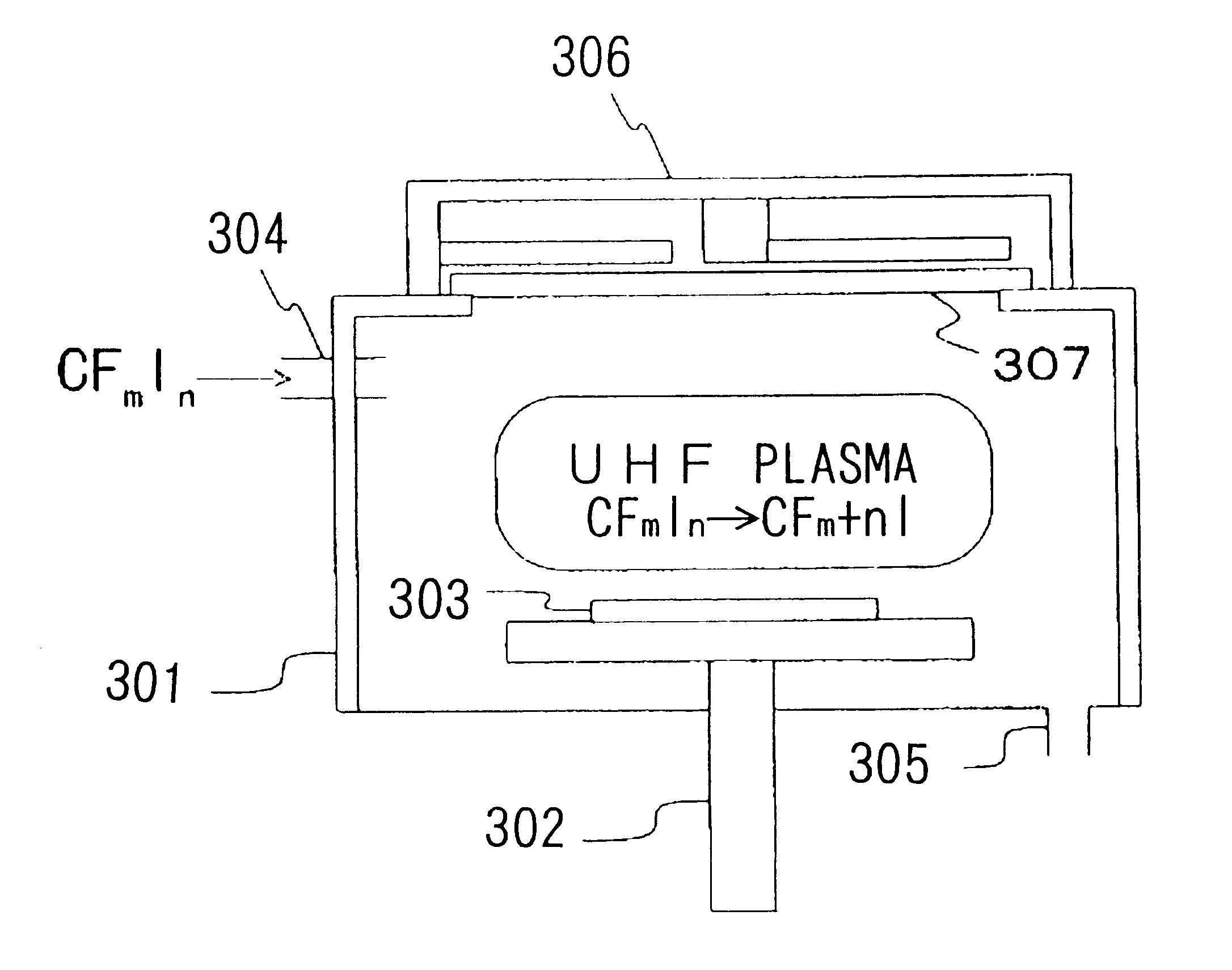
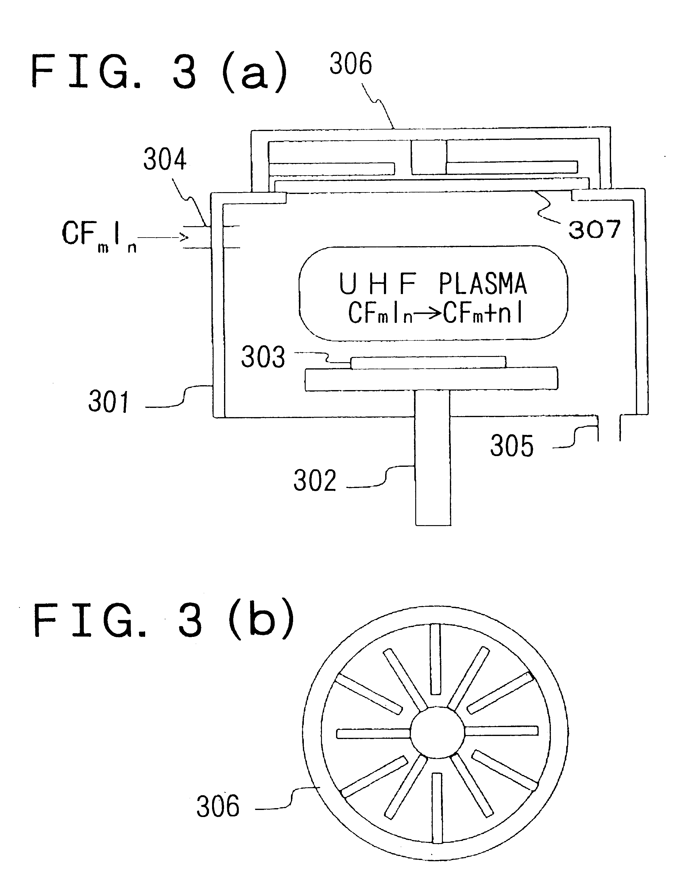
FIG. 3 shows a UHF plasma etching apparatus used in this example. This UHF plasma etching apparatus is equipped with a substrate holder 302 which also works as an electrode at the lower part of a vacuum chamber 301 made of stainless steel and a substrate 303 to be treated held on the substrate holder 302. A treating gas is introduced into the vacuum chamber 301 through an inlet 304 for charging the treating gas. The gas in the vacuum chamber is discharged through an outlet 305 by evacuating with a discharge pump which is not shown. On the vacuum chamber 301 a spoke antenna 306 opposed to the substrate holder 302 (electrode) is installed. This spoke antenna 306 is coupled to a treating r...
PUM
| Property | Measurement | Unit |
|---|---|---|
| Frequency | aaaaa | aaaaa |
| Frequency | aaaaa | aaaaa |
| Ratio | aaaaa | aaaaa |
Abstract
Description
Claims
Application Information


