Single crystal SiC and a method of producing the same

a single crystal, single crystal technology, applied in the direction of polycrystalline material growth, after-treatment details, gel state, etc., can solve the problems of leakage current, difficult to singly obtain a large-size single crystal, and low growth rate of about 1 mm/hr

Inactive Publication Date: 2001-03-20
NISSIN ELECTRIC CO LTD
View PDF2 Cites 12 Cited by
  • Summary
  • Abstract
  • Description
  • Claims
  • Application Information

AI Technical Summary

Benefits of technology

Furthermore, the heat treatment is performed under a state where the two complexes are piled via the surfaces of the polycrystalline films of the complexes, and particularly a state where the surfaces of the polycrystalline films are smoothly ground and the smooth surfaces are closely fixed to each other. This suppresses contamination which is caused by adhesion of suspended substances and the like in the vicinity of the surfaces of the polycrystalline films, to a minimum level. Moreover, even when the ambient atmosphere is varied during the heat treatment, a phenomenon by which the variation of the ambient atmosphere causes a surface portion of the polycrystalline films to decompose and disappear, or crystals deposited in the vicinity to adhere to the surfaces of the polycrystalline films can be suppressed to a minimum level. Therefore, impurities, micropipe defects, and the like do not substantially remain. Furthermore, contamination from the outside, and an effect of the variation of the ambient atmosphere during the heat treatment can be suppressed to a minimum level so that a large-size single crystal SiC which stably has very high quality is obtained with high productivity. Thus, it is possible to attain the effect of expediting the practical use of single crystal SiC which is superior in a large capacity, a high frequency, a high dielectric strength, and a high resistance to environments to existing semiconductor materials such as Si (silicon) and GaAs (gallium arsenide) and which is expected as a semiconductor material for a power device.

Problems solved by technology

In the Achison method of the above-described conventional production methods, however, a single crystal is grown slowly over a long time period, so that the crystal growth rate is as low as about 1 mm / hr.
Thus, it is difficult to singly obtain a large-size single crystal.
Such pin holes are called micropipe defects and cause a leakage current when a semiconductor device is fabricated.
Accordingly, there exists a problem in that a single crystal SiC having sufficiently good quality cannot be obtained.
In the Achison method and the sublimation and recrystallization method, moreover, it is very difficult from a technical point of view to maintain cleanness of the atmosphere in the vicinity of a growing crystal, thereby producing a problem in that the quality is impaired also by contamination from the outside in the vicinity of a single crystal.
These problems block a practical use of a single crystal SiC which has superior characteristics as compared with other existing semiconductor materials such as Si and GaAs as described above.

Method used


Image

  • Single crystal SiC and a method of producing the same
  • Single crystal SiC and a method of producing the same
  • Single crystal SiC and a method of producing the same

Examples


Embodiment Construction

Hereinafter, an embodiment of the present invention will be described with reference to the drawings.

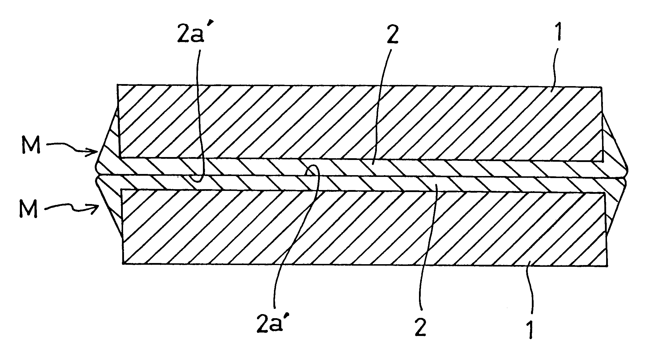
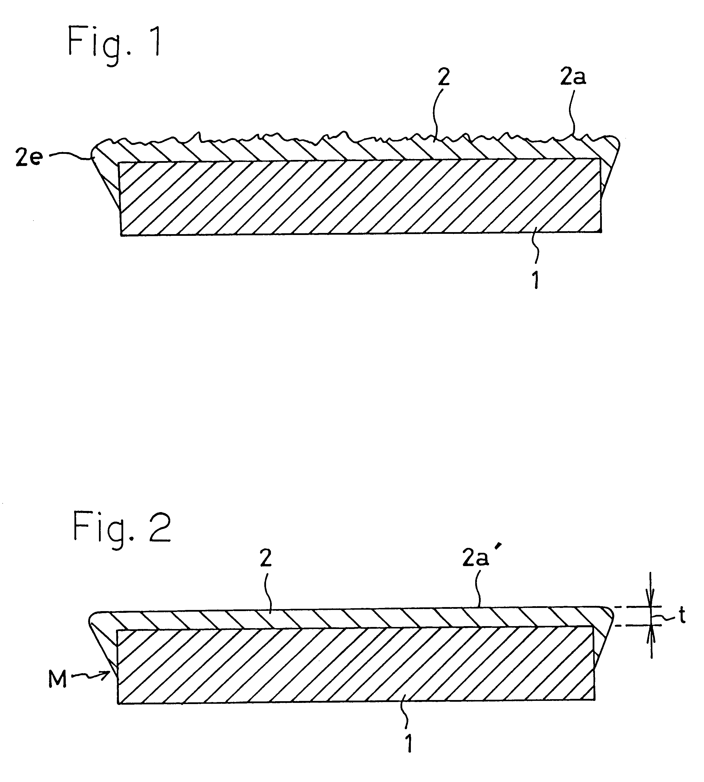
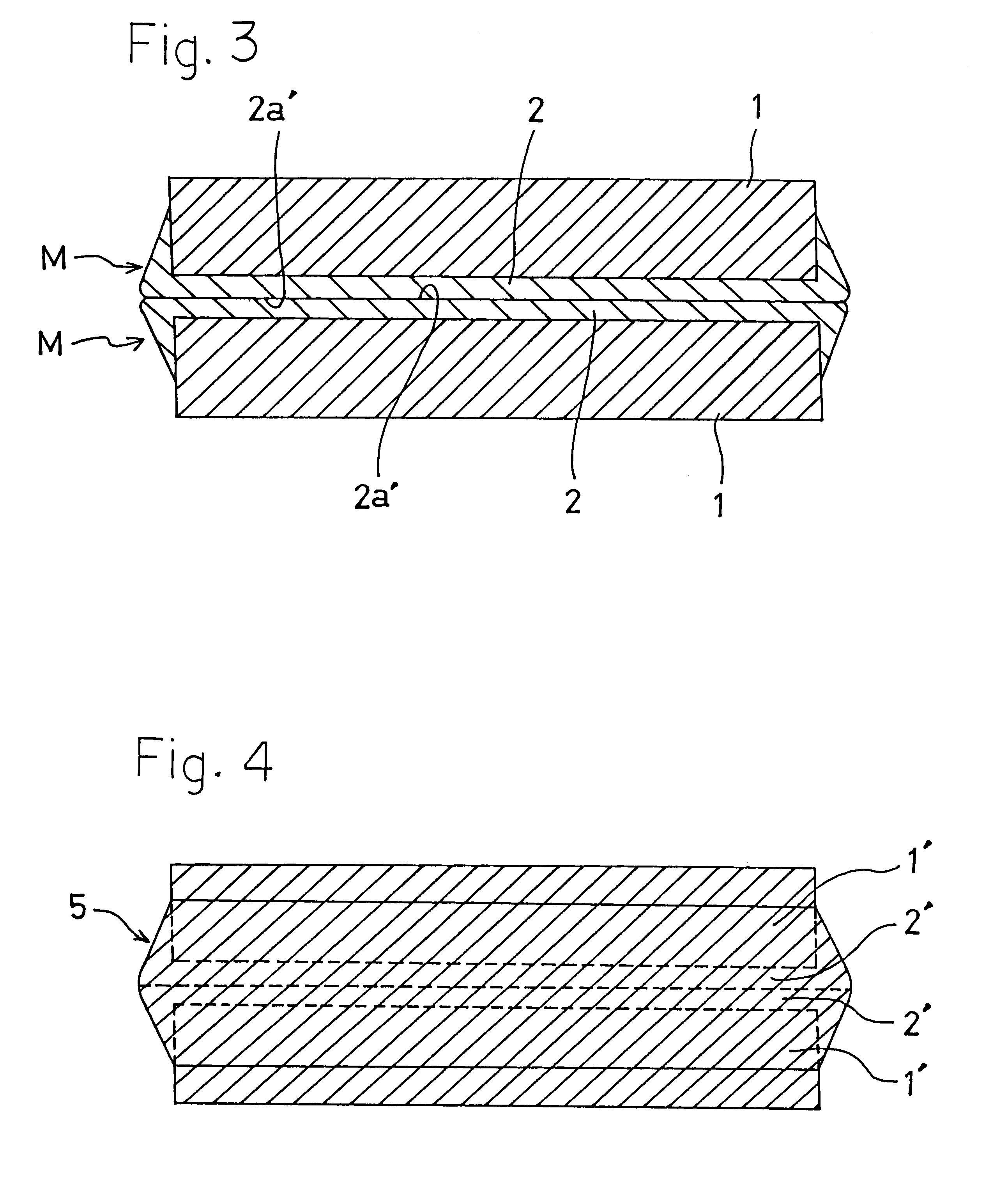
FIGS. 1 to 4 are schematic views illustrating the method of producing a single crystal SiC according to the invention, in the sequence of production steps. In FIG. 1, 1 denotes a single crystal hexagonal .alpha.-SiC substrate (6H type or 4H type). The single crystal .alpha.-SiC substrate 1 is produced by the sublimation and recrystallization method or the Achison method. A polycrystalline cubic .beta.-SiC film 2 is grown by thermochemical deposition in the range of 1,300 to 1,900.degree. C. so as to form an end portion 2e over the whole periphery of the side face of the single crystal .alpha.-SiC substrate 1.

Immediately after the film growth, as shown in FIG. 1, the surface 2a of the polycrystalline .beta.-SiC film 2 is in a rough face state where small irregularities are scattered. The surface 2a of the polycrystalline .beta.-SiC film 2 in the rough surface state is ground so that t...


PUM

PropertyMeasurementUnit
roughnessaaaaaaaaaa
roughnessaaaaaaaaaa
temperatureaaaaaaaaaa

Abstract

The single crystal SiC according to the present invention is produced in the following manner. Two complexes M in each of which a polycrystalline film 2 of beta-SiC (or alpha-SiC) is grown on the surface of a single crystal alpha-SiC substrate 1 by thermochemical deposition, and the surface 2a of the polycrystalline film 2 is ground so that the smoothness has a surface roughness of 200 angstroms RMS or smaller, preferably 100 to 50 angstroms RMS are subjected to a heat treatment under a state where the complexes are closely fixed to each other via their ground surfaces 2a', at a temperature of 2,000° C. or higher and in an atmosphere of a saturated SiC vapor pressure, whereby the polycrystalline films 2 of the complexes M are recrystallized to grow a single crystal which is integrated with the single crystal alpha-SiC substrates 1. Large-size single crystal SiC in which impurities, micropipe defects, and the like do not remain, and which has high quality can be produced with high productivity.

Description

1. Field of the InventionThe present invention relates to a single crystal SiC and a method of producing the same, and more particularly to a single crystal SiC which is used as a semiconductor substrate wafer for a light-emitting diode, an X-ray optical device such as a monochromatic sorter, a high-temperature semiconductor electronic element, and a power device, and also to a method of producing the single crystal SiC.2. Description of the Prior ArtSiC (silicon carbide) is superior in heat resistance and mechanical strength, and also has good resistance to radiation. In addition, it is easy to achieve valence control of electrons and holes by doping an impurity. Moreover, SiC has a wide band gap (for example, single crystal 6H--SiC has a band gap of about 3.0 eV, and single crystal 4H--SiC has a band gap of 3.26 eV). Therefore, it is possible to realize a large capacity, a high frequency, a high dielectric strength, and a high environmental resistance to which cannot be realized b...

Claims


Application Information

Patent Timeline
Patent Type & Authority Patents(United States)
IPC IPC(8): C30B25/18C30B25/02C30B1/00C30B29/36C30B33/02C30B33/06
CPCC30B1/00C30B25/02C30B25/18C30B29/36
Inventor TANINO, KICHIYAHIRAMOTO, MASANOBU
Owner NISSIN ELECTRIC CO LTD
Why Eureka
Try Eureka