Semiconductor device and method of fabricating the same

a technology of semiconductors and semiconductors, applied in semiconductor devices, electrical devices, transistors, etc., can solve the problems of increasing power consumption, hardly being able to form a channel formation region, and inability to specify the positions and sizes of crystal grains and forms

Inactive Publication Date: 2003-07-29
SEMICON ENERGY LAB CO LTD
View PDF11 Cites 99 Cited by
  • Summary
  • Abstract
  • Description
  • Claims
  • Application Information

AI Technical Summary

Problems solved by technology

In that case, it was impossible to specify the positions and sizes of the crystal grains and form them.
However, it has been hardly possible to form a channel formation region, in which the property of a crystal greatly influences the characteristics of a TFT, by a single crystal grain so as to exclude the influence of the crystal grain boundary.
Although it is possible to form a top gate type TFT by using the semiconductor film as an active layer in view of structure, since a parasitic capacitance is generated by the silicon oxide film provided between the semiconductor film and the high melting point metal layer, power consumption is increased and it becomes difficult to realize high speed operation of the TFT.
However, in the foregoing three-layer structure, even if the thickness of the semiconductor film is omitted, with respect to the thickness of the high melting point metal layer and the silicon oxide layer, since the thickness suitable for a crystallizing step is not necessarily coincident with the thickness suitable for the characteristics as a TFT element, it is impossible to simultaneously satisfy both the optimum design in the crystallizing step and the optimum design in the element structure.
Be

Method used


Image

  • Semiconductor device and method of fabricating the same
  • Semiconductor device and method of fabricating the same
  • Semiconductor device and method of fabricating the same

Examples


example 2

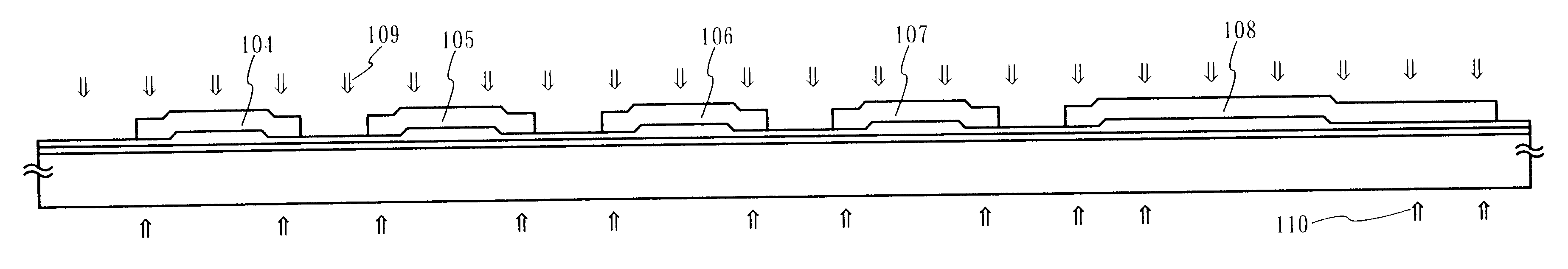
The active matrix substrate fabricated in the example 1 can be directly used for a reflection type liquid crystal display device. On the other hand, in the case of forming a transmission type liquid crystal display device, it is sufficient if a pixel electrode provided for each pixel of a pixel portion is formed of a transparent electrode. In this example, a method of fabricating an active matrix substrate corresponding to the transmission type liquid crystal display device will be described with reference to FIGS. 16A and 16B.

The active matrix substrate is fabricated similarly to the example 1. FIG. 16A shows a structure of a pixel portion thereof. FIG. 16A shows an example in which a transparent conductive film is first formed on a second interlayer insulating film, a patterning process and an etching process are carried out to form a pixel electrode 171, and then, a drain wiring line 172 is formed to partially overlap with the pixel electrode 171. As shown in FIG. 16B, a Ti film ...

example 3

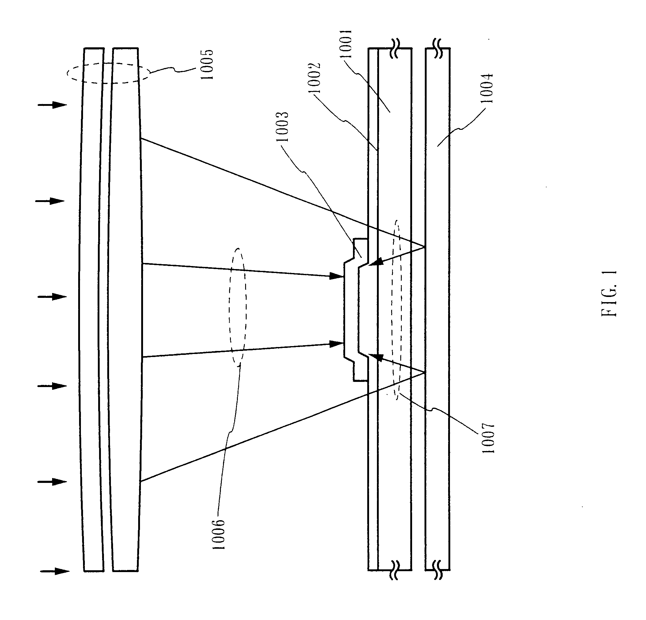
In a method of fabricating an island-like semiconductor layer having a crystal structure from an island-like semiconductor layer having an amorphous structure by the dual beam laser annealing method of the present invention, a trace amount (about 1.times.10.sup.17 to 1.times.10.sup.19 / cm.sup.3) of catalytic element used for crystallization remains in the island-like semiconductor layer having the crystal structure fabricated by the method of the embodiment 2. Of course, although a TFT can be completed even in such a state, it is preferable to remove the remaining catalytic element from at least a channel formation region. As one of means for removing this catalytic element, there is a means using the gettering function of phosphorus (P).

A gettering process by phosphorus (P) for this object can be carried out in parallel with the activation step explained in FIG. 12A. This state will be described with reference to FIG. 17. The concentration of phosphorus (P) required for gettering m...

example 4

In this example, a process of fabricating an active matrix type liquid crystal display device from an active matrix substrate fabricated in the example 1 will be described. As shown in FIG. 18, columnar spacers 901 and 902 are formed on the active matrix substrate in the state of FIG. 12B. Although a method of dispersing particles of several .mu.m to provide the spacers may be used, the columnar spacers may be formed like this by forming a resin film on the entire surface of the substrate and patterning this. Although the material of such columnar spacers is not restricted, for example, NN700 made by JSR Co., Ltd. is used, and after it is applied by a spinner, an exposure and a developing process are carried out to form a predetermined pattern. Further, heating at 150 to 200.degree. C. is carried out by a clean oven or the like to harden it. Although the shape of the columnar spacer fabricated in this way can be changed by conditions of the exposure and developing process, if the sh...


PUM


Abstract

A crystalline semiconductor film in which the position and size of a crystal grain is controlled is fabricated, and the crystalline semiconductor film is used for a channel formation region of a TFT, so that a high performance TFT is realized. An island-like semiconductor layer is made to have a temperature distribution, and a region where temperature change is gentle is provided to control the nucleus generation speed and nucleus generation density, so that the crystal grain is enlarged. In a region where an island-like semiconductor layer 1003 overlaps with a base film 1002, a thick portion is formed in the base film 1002. The volume of this portion increases and heat capacity becomes large, so that a cycle of temperature change by irradiation of a pulse laser beam to the island-like semiconductor layer becomes gentle (as compared with other thin portion). Like this, a laser beam is irradiated from the front side and reverse side of the substrate to directly heat the semiconductor layer, and heat conduction from the semiconductor layer to the side of the substrate and heat conduction of the semiconductor layer in the horizontal direction to the substrate are used, so that the increase in the size of the crystal grain is realized.

Description

1. Field of the InventionThe present invention relates to a method of fabricating a semiconductor film having a crystal structure and formed on a substrate having an insulating surface, and a method of fabricating a semiconductor device using the semiconductor film as an active layer. Particularly, the present invention relates to a method of fabricating a thin film transistor in which an active layer is formed of a crystalline semiconductor layer. Incidentally, in the present specification, the term "semiconductor device" indicates all devices capable of functioning by using semiconductor characteristics, and includes, in its category, an electro-optical device typified by an active matrix type liquid crystal display device formed by using thin film transistors, and an electronic equipment incorporating that kind of electro-optical device as a part.2. Description of the Related ArtThere has been developed a thin film transistor (hereinafter referred to as a TFT) in which an amorpho...

Claims


Application Information

Patent Timeline
IPC IPC(8): H01L21/70H01L27/12H01L21/84H01L21/77H01L27/13H01L29/786
CPCH01L29/78603H01L27/1255H01L27/1277H01L27/1281
Inventor KAWASAKI, RITSUKOKASAHARA, KENJIOHTANI, HISASHI
Owner SEMICON ENERGY LAB CO LTD
Why Eureka
Try Eureka