

Optical device, a fabrication method thereof, a driving method thereof and a camera system
- Summary
- Abstract
- Description
- Claims
- Application Information
AI Technical Summary
Benefits of technology
Problems solved by technology
Method used
Image

Examples
first embodiment
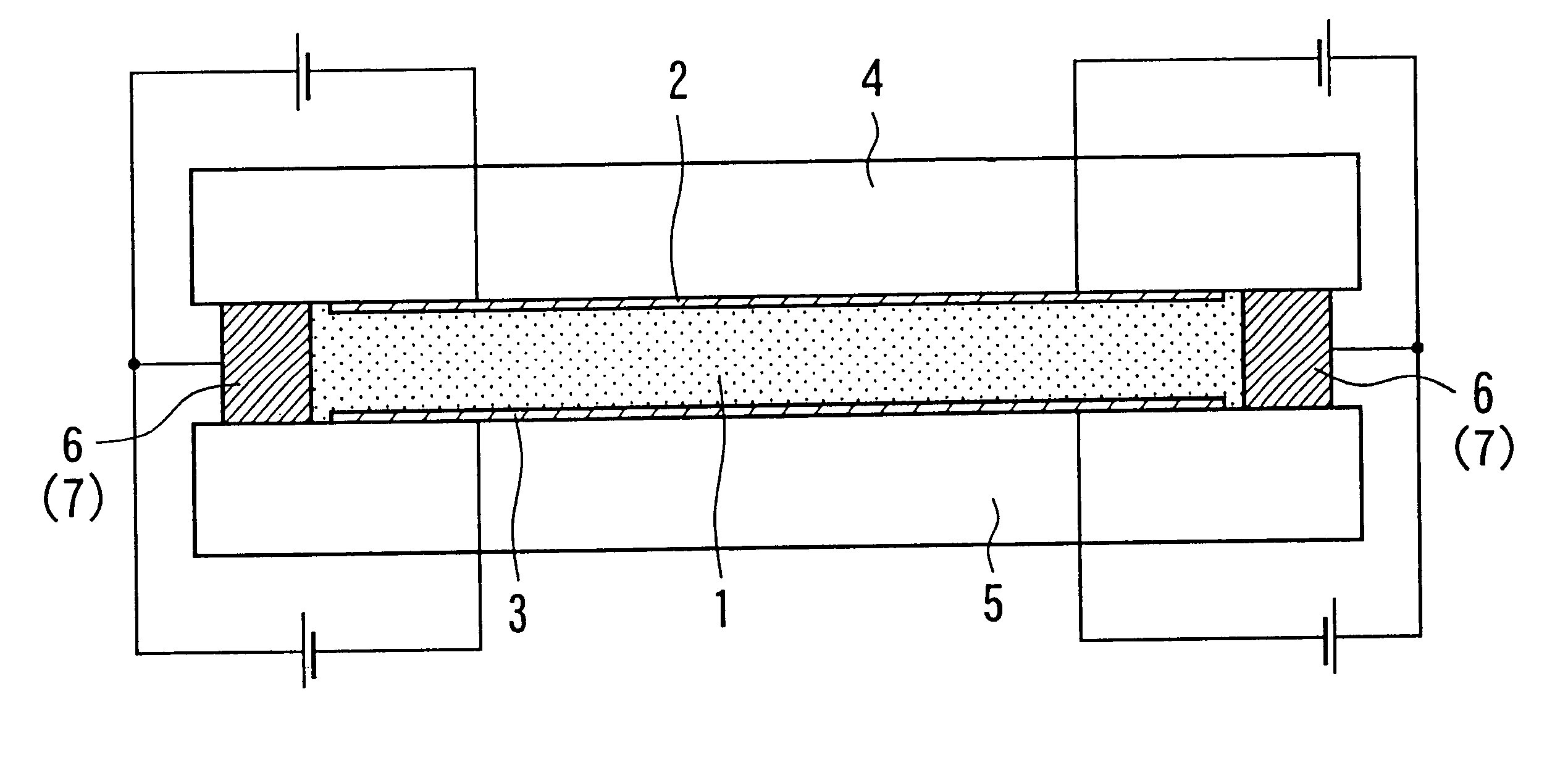
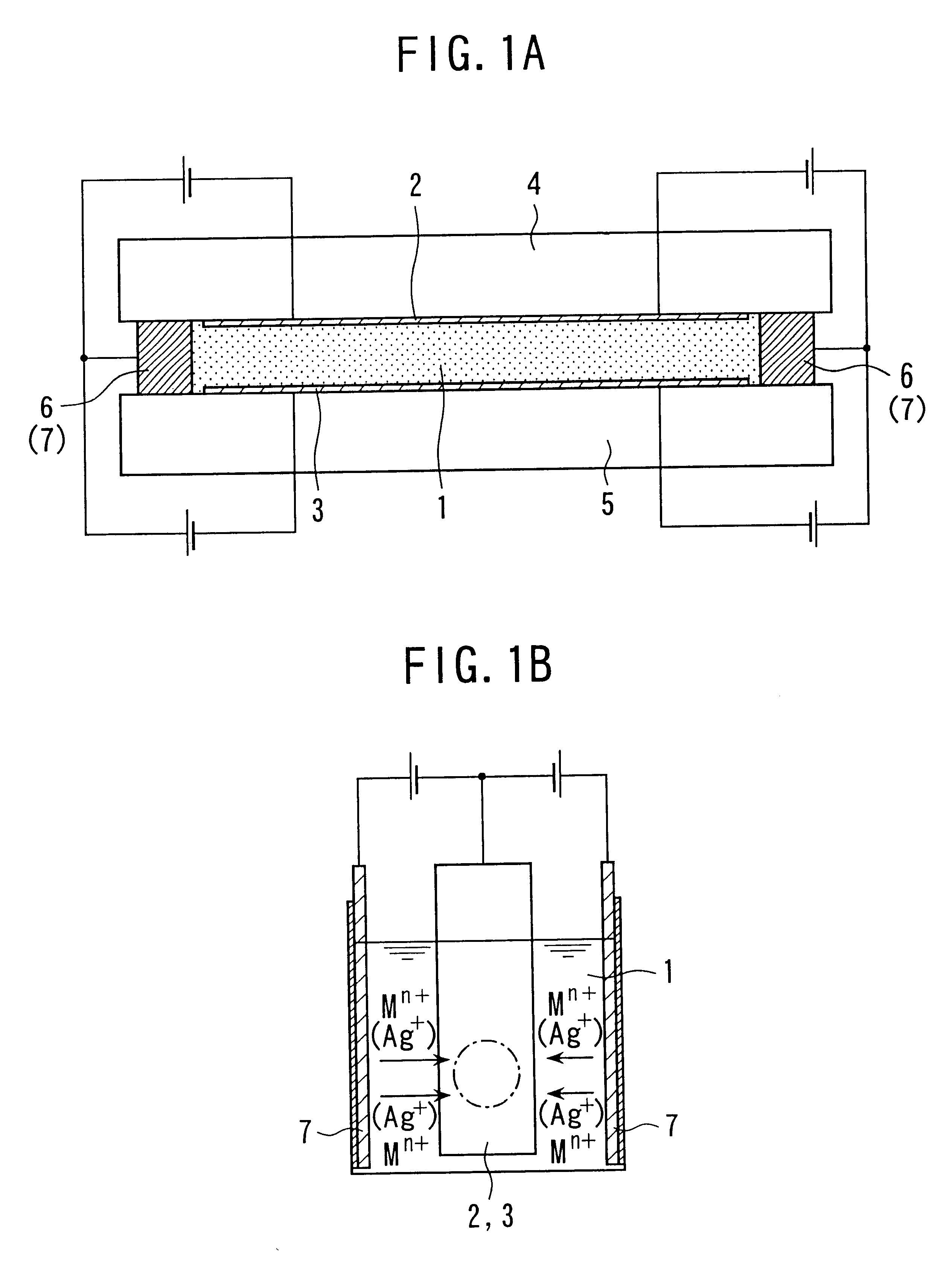
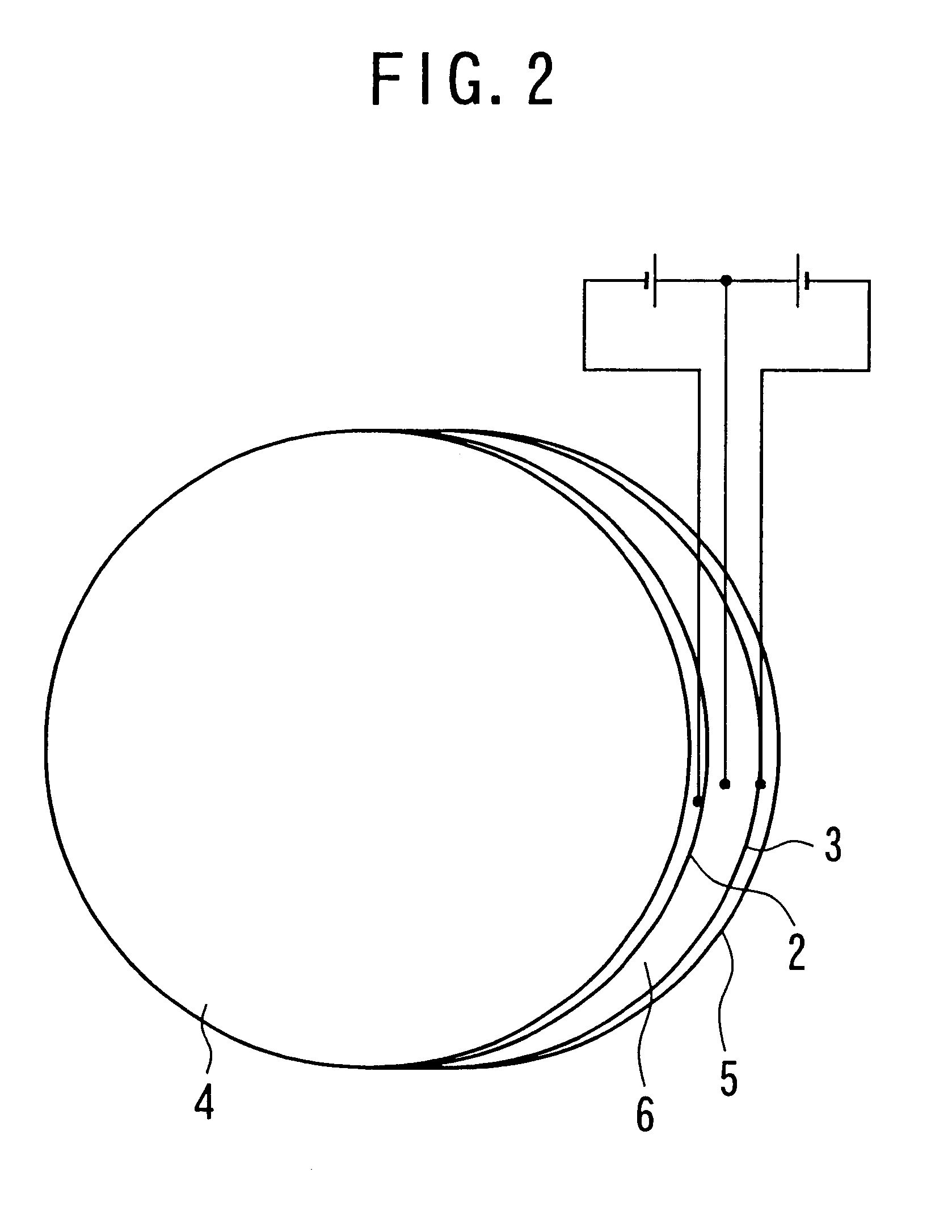
An optical device and a fabrication method for the present invention can be applied suitably to an optical device comprising a working electrode, a counter electrode and an electrolyte disposed in contact with both of the electrodes, wherein the working electrode has a transmissivity of 70% or more in a visible light region, a material including a metal is electrodeposited on the working electrode and thereby light is electrochemically controlled by an electric field to the electrolyte.
In an optical device for a first embodiment of the present invention, at least a lead electrode for an electrode, a particularly transparent electrode is covered with a cover layer containing at least one layer of insulation material. Further, a fabrication method of the optical device is preferably conducted such that at least the entire surface of the transparent electrode is covered with a cover layer containing at least one layer of an insulation material and the cover layer is removed only from t...
second embodiment
An optical device and a fabrication method for the present invention can be applied suitably to an optical device comprising a working electrode, a counter electrode and an electrolyte disposed in contact with both of the electrodes, wherein the working electrode includes a transmissivity of 70% or more in a visible light region, a material including a metal is electrodeposited on the working electrode from the electrolyte and thereby light is controlled electrochemically by an electric field to be applied to the electrolyte.
The working electrode according to the present invention comprises an oxide layer in which indium is doped to tin, wherein indium / tin is 1.5 or less by element ratio. The optical device has an excellent spectrum characteristic.
However, an electrical resistance of the oxide layer gets larger as tin ratio increases. Particularly, when indium / tin is less than 0.5, the electrical resistance increases abruptly. A large electrical resistance causes a large polarizatio...
third embodiment
Also an optical device and a fabrication method of a third embodiment according to the present invention can be applied suitably to an optical device comprising a working electrode as an electrode having a transmissivity of 70% or more in a visible light region, a counter electrode and an electrolyte disposed in contact with both of the electrodes in which light is electrochemically controlled by an electric field applied to the electrolyte.
In this case, it is preferred that a tin oxide layer is laminated to a thickness of 5 nm or more and 130 nm or less, preferably, from 5 nm to 10 nm so as to cover the oxide layer in which indium is doped to tin constituting the working electrode.
Further, the tin oxide layer is preferably formed by a gas phase film forming method and the layer can be formed suitably by using a sputtering, physical vapor deposition or chemical gas phase growing method as the gas phase film forming method.
This enables to drive preferably an optical device comprising...
PUM
 Abstract
Description
Claims
Application Information