Semiconductor wafer with ultra thin doping level formed by defect engineering

a technology of defect engineering and semiconductors, applied in the direction of semiconductor devices, electrical equipment, basic electric elements, etc., can solve the problems of inability to solve, the current of the implanter is significantly reduced, and the output is not high, and achieves high levels of vacancies

Inactive Publication Date: 2004-11-02
CHU WEI KAN
View PDF12 Cites 11 Cited by
  • Summary
  • Abstract
  • Description
  • Claims
  • Application Information

AI Technical Summary

Benefits of technology

A preferred embodiment of the invention is to cool the wafer rapidly from a high temperature so that the high levels of vacancies and interstitials formed in equilibrium are "frozen in". The interstitials are much more mobile than the

Problems solved by technology

Furthermore, the conventional ion implantation techniques used to dope submicron silicon devices have throughput problems attributed to the fact that an ion beam implanter current drops significantly due to space charge limitations at very low ion energy.
However, all of them have the disadvantage that they cannot solve the most serious problem, the spreading of the dopant profiles due to the transient enhanced diffusion and boride-enhanced diffusion (BED).
BED is a greater problem than TED because high concentrations of boron are necessary in any doping method used.
in. Although carbon co-implant is effective in reducing the transient diffusion of boron, this method suffers from the disadv

Method used


Image

  • Semiconductor wafer with ultra thin doping level formed by defect engineering
  • Semiconductor wafer with ultra thin doping level formed by defect engineering
  • Semiconductor wafer with ultra thin doping level formed by defect engineering

Examples


example 1

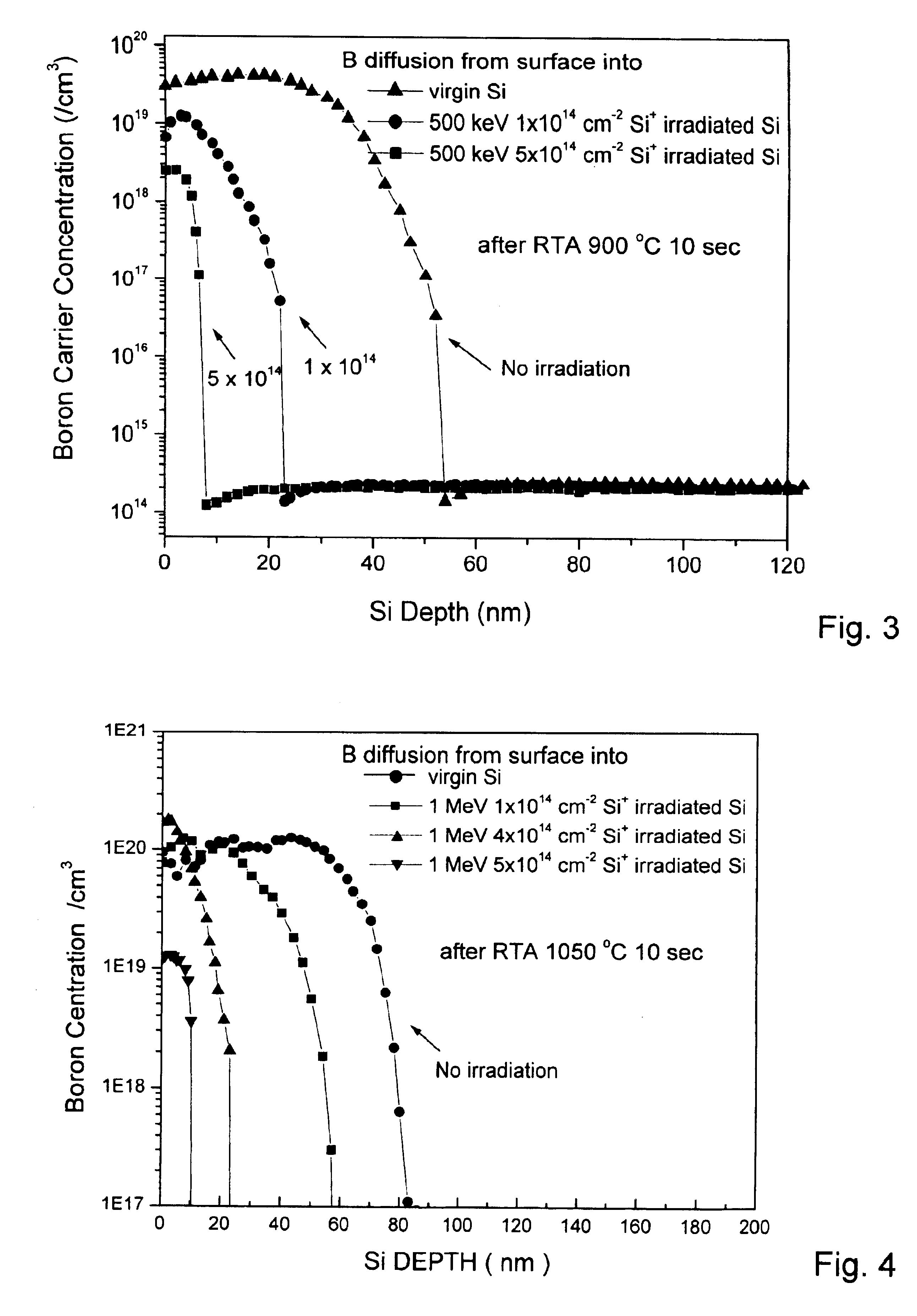
n-type (100) Czochralski-grown Si wafers were first implanted with 500 keV Si ions to a dose of 1.times.10.sup.14 or 5.times.10.sup.14 / cm.sup.2, respectively, followed by an HF etch to remove the native oxide and then by deposition of a 10 nm layer of boron. A liquid nitrogen cooled substrate holder was used to hold the wafer during the boron deposition to decrease the mobility of the deposited boron atoms to avoid boron island formation. A layer about 4 nm thick was uniformly deposited. After the deposition, Si wafers were rapid thermal annealed at 900.degree. C. for 10 sec. FIG. 3. shows a graph of a typical spreading resistance profiles of samples first implanted with 500 keV Si ions to a dose of 1.times.10.sup.14 or 5.times.10.sup.14 / cm.sup.2 respectively, followed by deposition of a 10 nm layer of boron, and annealing

example 2

n-type (100) Czochralski-grown Si wafers were first implanted with 1 MeV Si ions with doses of 1.times.10.sup.14 / cm.sup.2, 4.times.10.sup.14 / cm.sup.2 and 5.times.10.sup.14 / cm.sup.2 respectively, then a thin boron layer was deposited on the cooled wafer by by e-gun deposition. Subsequent annealing was at 1050.degree. C. for 10 sec.

FIG. 4 shows a graph of typical spreading resistance profiles of boron doped silicon.

example 3

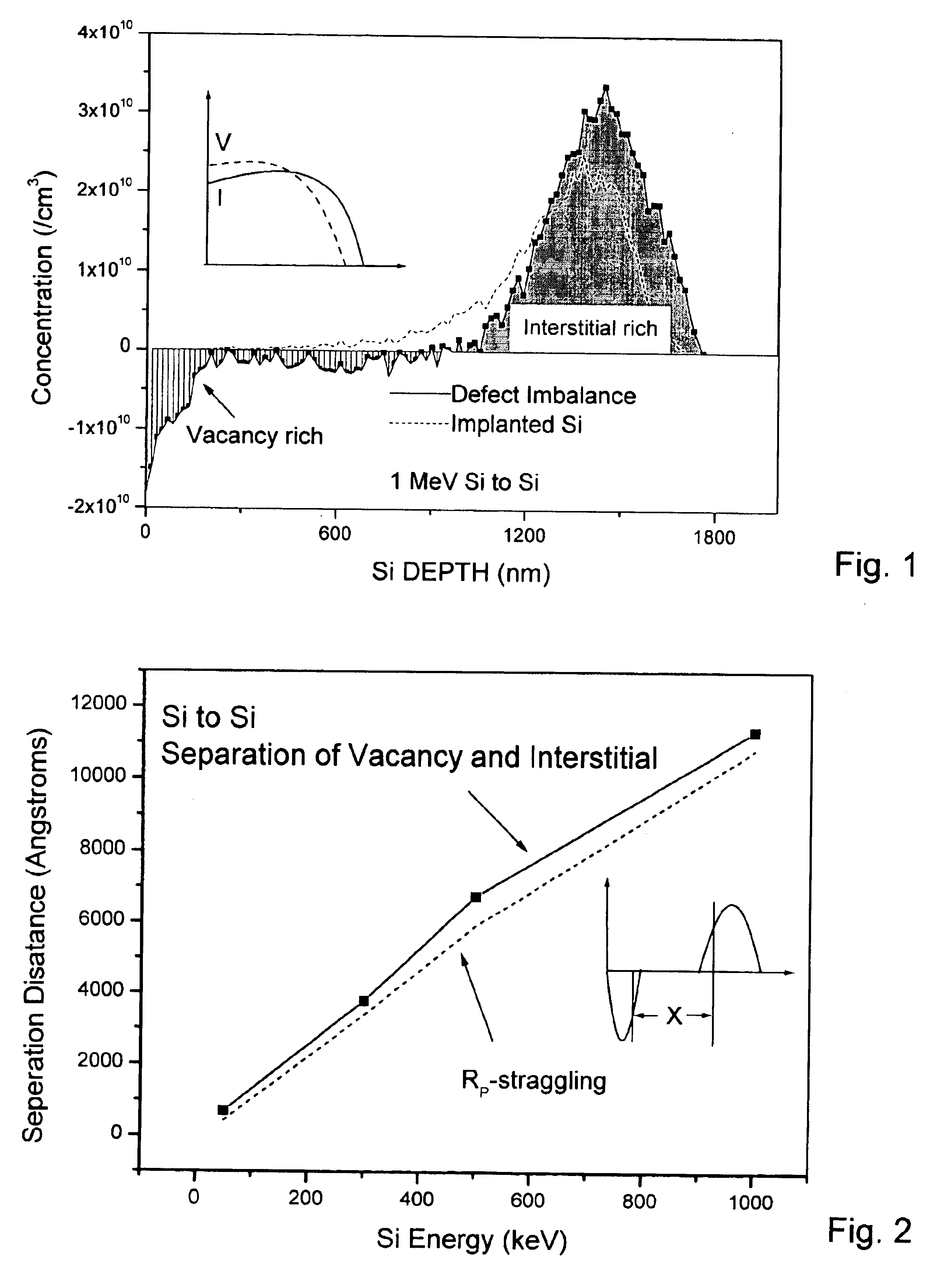
n-type (100) Czochralski-grown Si wafers were first implanted with 5.times.10.sup.14 / cm.sup.2 of Si.sup.+ ions with incident energies of 50 keV or 500 keV, and then a 10 nm thick boron layer was deposited onto the cooled surface of the Si substrate. The samples were subsequently annealed at 900.degree. C., 950.degree. C. and 1050.degree. C. for 15 sec. Using higher energy bombardment such as 500 keV to get a larger separation of vacancies and interstitials, boron diffusion was further suppressed over that of 50 keV implanted sample.

FIG. 5 shows a graph of typical secondary ion mass spectrometry (SIMS) depth profiles of boron diffused from a surface deposited layer into an high energy ion implantation damaged Si substrate.


PUM


Abstract

Vacancies and dopant ions are introduced near the surface of a semiconductor wafer. The dopant ions which diffuse by an interstitialcy mechanism have diffusivity greatly reduced, which leads to a very low resistivity doped region and a very shallow junction.

Description

The present invention relates generally to the field of semiconductor manufacturing, and more particularly to ultra shallow junction formation in Si by defect engineering, and to apparatuses for their practice.Complementary metal-oxide-semiconductor (CMOS) technology has continued to evolve for the past 40 years with integrated circuit (IC) density quadrupling every three years to reduce cost and improve device performance (e.g. speed). Denser circuits need device scaling with requirement of increasingly compact (shallow and rapidly varying) doping profiles in both the source / drain junctions. The International Technology Roadmap for Semiconductors (ITRS) anticipates junctions around 25 nanometers (nm) deep, with sheet resistance of 250 Ohm / square for the 100 nm lithography technology generation. Junctions this shallow have approached the process limits of conventional implantation and thermal annealing processes. It is well known that boron dopants experience transient enhanced diff...

Claims


Application Information

Patent Timeline
IPC IPC(8): H01L21/225H01L21/265H01L21/02H01L29/02H01L29/34
CPCH01L21/2254H01L21/2257H01L29/34H01L21/26513H01L21/26506H01L21/26566
Inventor CHU, WEI-KANSHAO, LINLU, XINMINGLIU, JIARUIWANG, XUEMEI
Owner CHU WEI KAN
Why Eureka
Try Eureka