Semiconductor element and semiconductor device comprising the same

a semiconductor and semiconductor technology, applied in the direction of semiconductor devices, electrical devices, transistors, etc., can solve the problems of affecting the operation of the semiconductor device, and unable to obtain crystal orientation without deviation, etc., to achieve high current driving, high-speed operation, and little variation among the pluralities of elements

Inactive Publication Date: 2005-01-25
SEMICON ENERGY LAB CO LTD
View PDF29 Cites 46 Cited by
  • Summary
  • Abstract
  • Description
  • Claims
  • Application Information

AI Technical Summary

Benefits of technology

[0026]By specifying a semiconductor element such as a transistor or especially the region where a channel formation region is formed, it becomes possible to form a crystalline semiconductor region having no grain boundary existing therein. By the above, factors of variation in characteristics due to a crystal grain boundary which intervenes improperly or crystal defects, can be eliminated. That is, a semiconductor element or the semiconductor element group that has capabilities of high current driving, high-speed operation, and little variation among pluralities of elements can be achieved.
[0027]The depression in no fewer than 0.01 μm to nor more than 2 μm in width, and in no fewer than 0.01 μm to nor more than 3 μm in depth make it possible to form a semiconductor region having high aspect ratio in linear stripe pattern. In the present invention, taking advantage of the characteristics, we use the semiconductor region having high aspect ratio as other electrode of the capacitor element. It makes possible to increase an effective surface area per unit area, then, the capacitance element may have high-density electric charge requiring a small area. Thus, the capacitance element included in the semiconductor device of the present invention is formed from a plurality of the first crystalline semiconductor region provided in parallel, the insulating film covering the plurality of the first crystalline semiconductor region, and wirings opposing to the crystalline semiconductor region by sandwiching the insulating film.

Problems solved by technology

However, when crystallization is made by irradiating the laser beams onto the amorphous semiconductor film formed on the flat surface, the crystal was made into poly-crystals, producing defects such as a grain boundary which was formed improperly.
Therefore, crystal orientations without deviation could not be obtained.
Crystal defects are involved in a grain boundary, resulting in a carrier trap.
Accordingly, if special methods such as bond-and-etchback SOI (Silicon on Insulator) are excluded, the crystallized or re-crystallized crystalline semiconductor films formed on an insulating surface, could not obtain an equivalent quality to a MOS transistor which is formed on a single crystal substrate.
However, it was almost impossible to arrange a transistor so as to obviate a grain boundary formed improperly.
That is, the grain boundary or crystal defects involved therein unexpectedly could not be eliminated by controlling the crystallinity of the channel formation regions of a transistor strictly.
Especially when crystalline semiconductor films are formed on a non-alkali glass substrate currently used abundantly industrially by using laser beams, the focus of the laser beams varies in response to the influence of the surge of the non-alkali glass substrate itself, involving a problem of causing crystalline variation as a result.

Method used


Image

  • Semiconductor element and semiconductor device comprising the same
  • Semiconductor element and semiconductor device comprising the same
  • Semiconductor element and semiconductor device comprising the same

Examples


embodiment

[0090 Mode 1

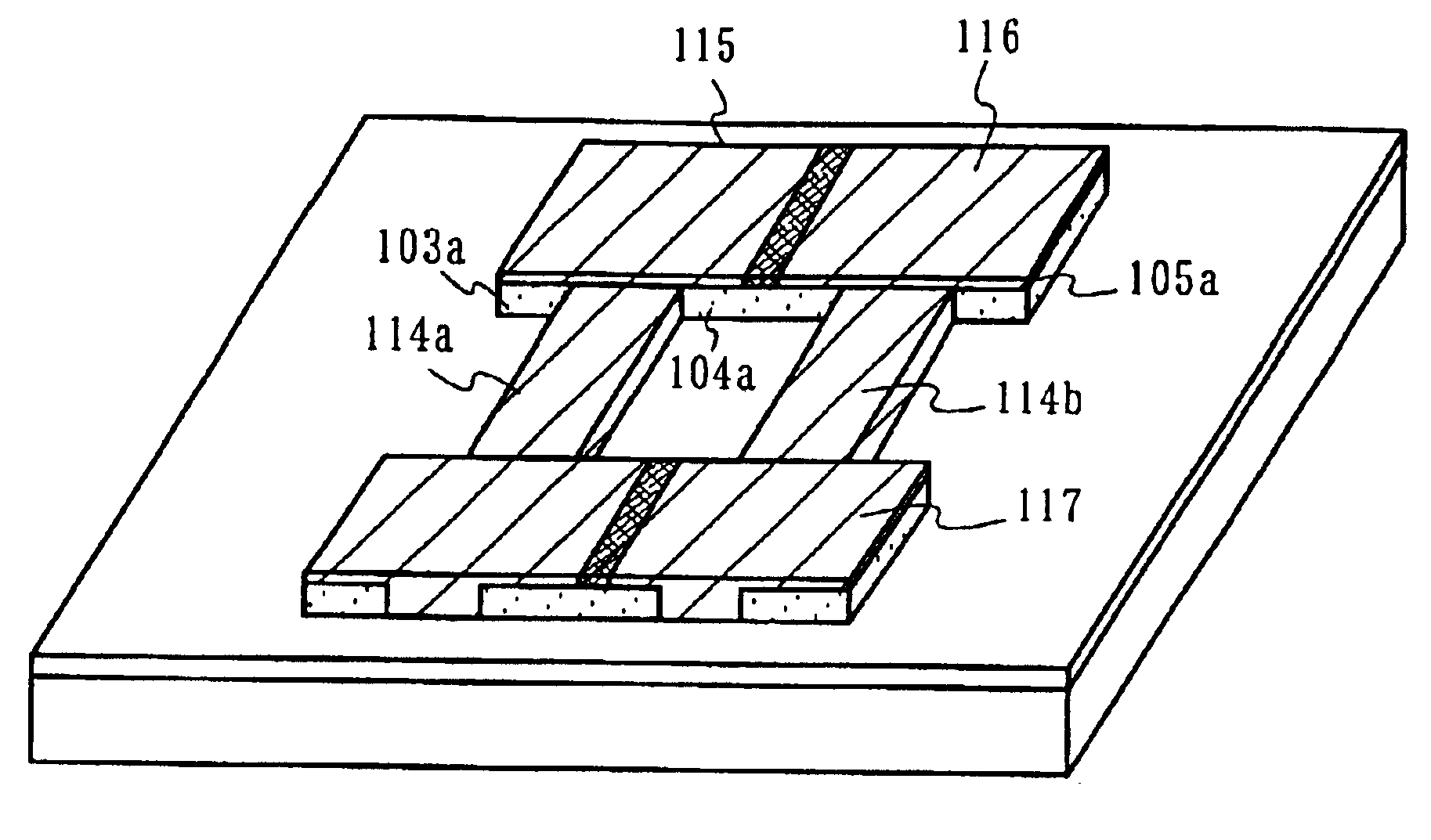
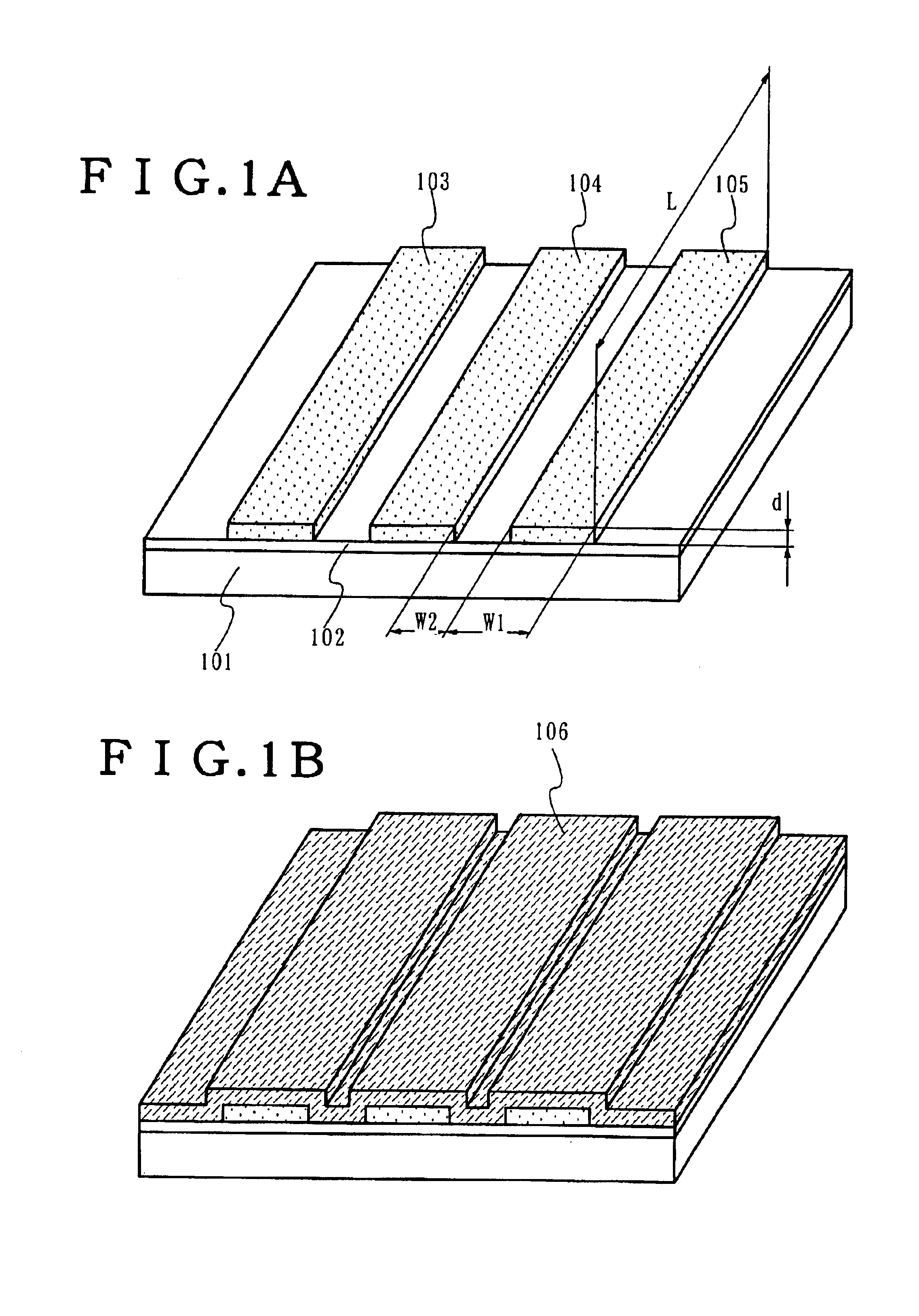
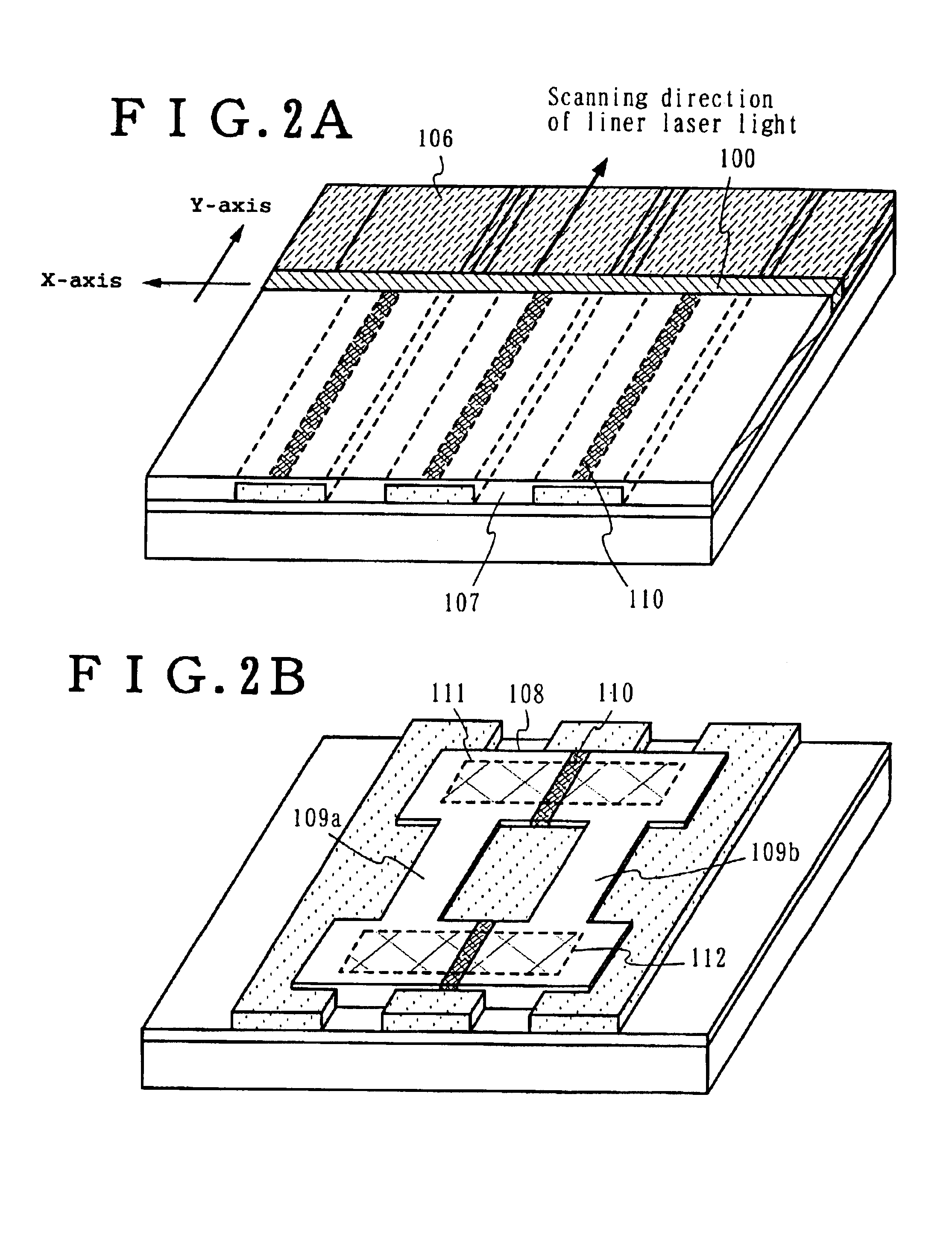
[0091]Aspects of the embodiment of manufacturing method for a thin film transistor using the present invention will be explained in the following with reference to the drawings. The perspective diagram shown in FIG. 1A shows the film formation where first insulating film 102 and second insulating films 103 to 105 formed in linear stripe pattern are formed on substrate 101. Three linear stripe patterns formed by the second insulating film are shown in FIG. 1A. However, the number thereof is not limited to this.

[0092]As for substrates, a substrate covering the surface of a commercial non-alkali glass substrate, a quartz substrate, a sapphire substrate, a single crystal, or a poly-crystalline semiconductor substrate with an insulating film, and a substrate covering the surface of a metal board with an insulating film can be applied. For forming a linear stripe pattern with a submicron design rule, it is desirable to set the irregularities on the surface of the substrate, su...

embodiment 1

[0302

[0303]A crystalline semiconductor film obtained by implementing this invention is shown in this embodiment. In addition, since the crystallization process was performed according to Embodiment modes 2 and 3, this embodiment mode is described with reference to FIGS. 6A to 8E.

[0304]In this embodiment mode, a silicon nitride oxide film with thickness of 50 nm was used as first insulating film 302 in FIGS. 6A-D, and a silicon oxynitride film with thickness of 200 nm was used as second insulating film 303. In this case, since the first insulating film 302 of a base film was subjected to etching when the second insulating film 303 was also subjected to etching, resulting in obtaining the height of 250 nm equivalent to the level difference d shown FIG. 1. Moreover, width of the second insulating film 303 (it is equivalent to W1 in FIG. 1) was set to 0.5 μm, and distance between contiguity (it is equivalent to W2 in FIG. 1) was set to 0.5 μm.

[0305]Moreover, after a silicon oxynitride f...

embodiment 2

[0310

[0311]In this embodiment, an example will be described in which, in forming the second insulating films 103 to 105 shown in FIGS. 1A-B, an insulating film equivalent to a first insulating film is formed on the second insulating films 103 to 105 using a glass substrate as an etching stopper.

[0312]In FIG. 39, first, second insulating films 853 to 855 are formed of silicon oxide or silicon oxide nitride with a thickness of 10 to 3000 nm, preferably 100 to 2000 nm in a linear stripe pattern on a glass substrate851. Details are the same as Embodiment mode 1. As a method of etching, etching using buffer fluoric acid or dry etching using CHF3 is adopted. In this embodiment, the dry etching using a CHF3 gas is adopted. In this case, it is sufficient that a gas flow amount is 30 to 40 sccm, a reactive pressure is 2.7 to 4.0 Kpa, an applied power is 500 W, and a substrate temperature is 20° C.

[0313]In addition, in the case of this embodiment, as the glass substrate 851, it is preferable ...


PUM


Abstract

A semiconductor element which is capable of operating at a high speed, high in an electric current drive capability, and small in fluctuation among a plurality of elements, and a semiconductor device including the semiconductor element are provided. The semiconductor element has a first crystalline semiconductor region including plural crystal orientations without practically having a grain boundary on an insulating surface, the first crystalline semiconductor region being provided to be jointly connected to a conductive region including the first crystalline semiconductor region and a second crystalline semiconductor region, in which the conductive region is provided astride insulating films extending in a linear stripe pattern.

Description

BACKGROUND OF THE INVENTION[0002]The present invention relates to a semiconductor element formed using a semiconductor film having a crystal structure and a method for manufacturing the same, and relates to a semiconductor device having a circuit which integrated the semiconductor element and a method for manufacturing the same. This invention especially relates to a thin film diode or the like using a field-effect transistor (Typically Thin-Film Transistor) and a crystalline semiconductor film.[0003]Technology for forming semiconductor elements such as a transistor by crystallizing an amorphous silicon film that was formed on an insulating substrate of glass or the like is developed. Especially the technology for irradiating laser beams and crystallizing the amorphous silicon film is applied to the manufacture technology of a thin-film transistor (TFT). A transistor produced using semiconductor films (crystalline semiconductor films) with crystal structure is applied to a plane typ...

Claims


Application Information

Patent Timeline
Patent Type & Authority Patents(United States)
IPC IPC(8): H01L21/02H01L29/786H01L21/20H01L29/66H01L21/70H01L21/336H01L27/12H01L21/84H01L21/77
CPCH01L21/2026H01L27/12H01L29/66757H01L27/1281H01L29/78675H01L29/78696H01L29/78621H01L21/02686H01L21/02683H01L21/02502H01L21/02678H01L21/02422H01L21/02488H01L21/02532H01L21/0242H01L21/02672H01L21/02691H01L21/02609
Inventor YAMAZAKI, SHUNPEIKATO, KIYOSHIISOBE, ATSUOMIYAIRI, HIDEKAZUSUZAWA, HIDEOMISHIONOIRI, YUTAKAMIYAKE, HIROYUKI
Owner SEMICON ENERGY LAB CO LTD
Why Eureka
Try Eureka