Semiconductor device and manufacturing method thereof

Inactive Publication Date: 2005-02-15
SEMICON ENERGY LAB CO LTD
View PDF62 Cites 133 Cited by
  • Summary
  • Abstract
  • Description
  • Claims
  • Application Information

AI Technical Summary

Benefits of technology

[0008]Conventionally, the production costs have been high in order to manufacture a TFT on a substrate with a technique of photolithography using at least 5 photomas

Problems solved by technology

Conventionally, the production costs have been high in order to manufacture a TFT on a substrate with a technique of photolithography using at least 5 photomasks for an active matrix type electro-optical device.
Therefore, the entire process becomes complex, which leads to a problem.
Further, static electricity is generated by causes such as friction during manufacturing steps because the substrate is an insulator.
If static el

Method used


Image

  • Semiconductor device and manufacturing method thereof
  • Semiconductor device and manufacturing method thereof
  • Semiconductor device and manufacturing method thereof

Examples


embodiment 1

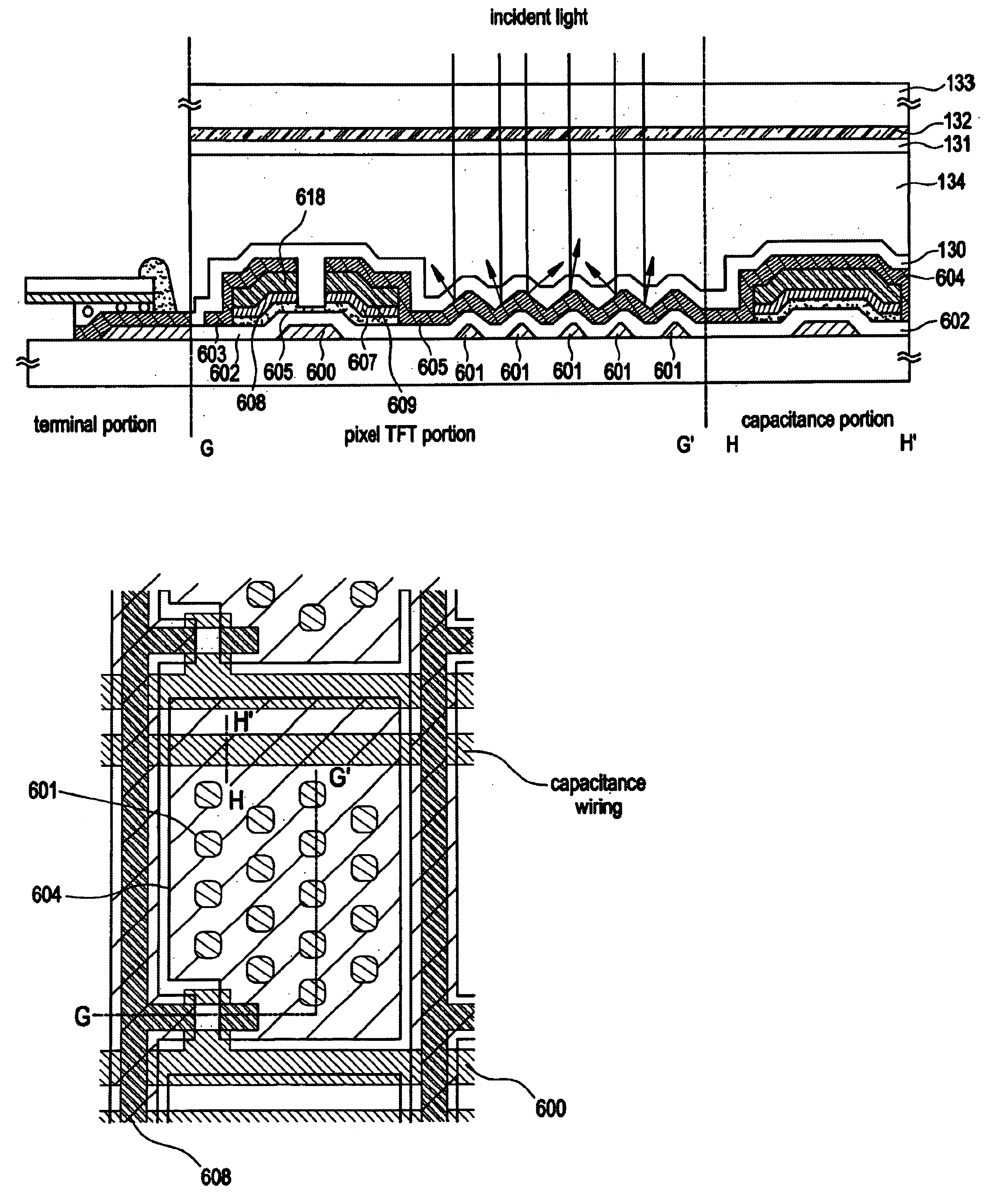
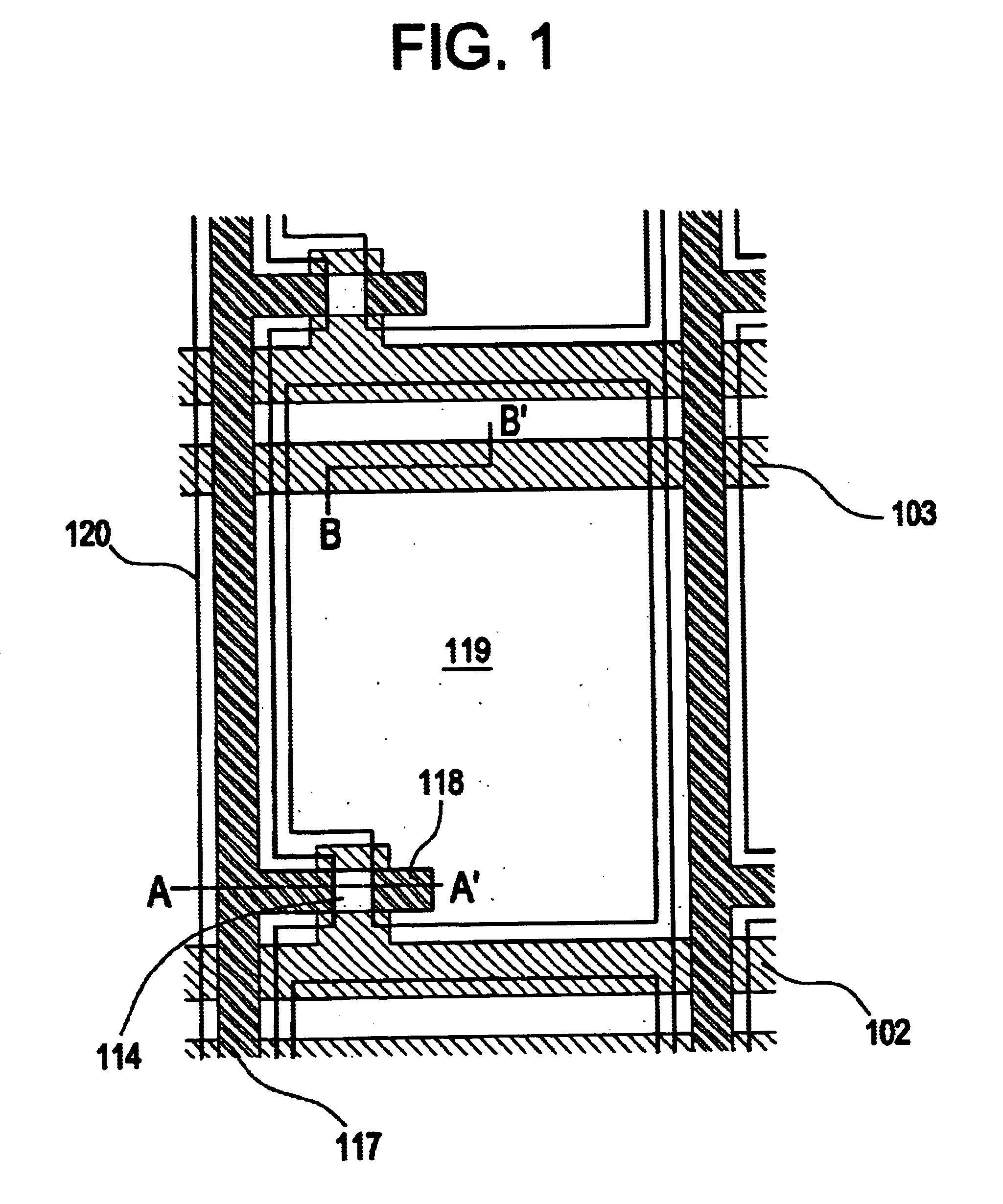
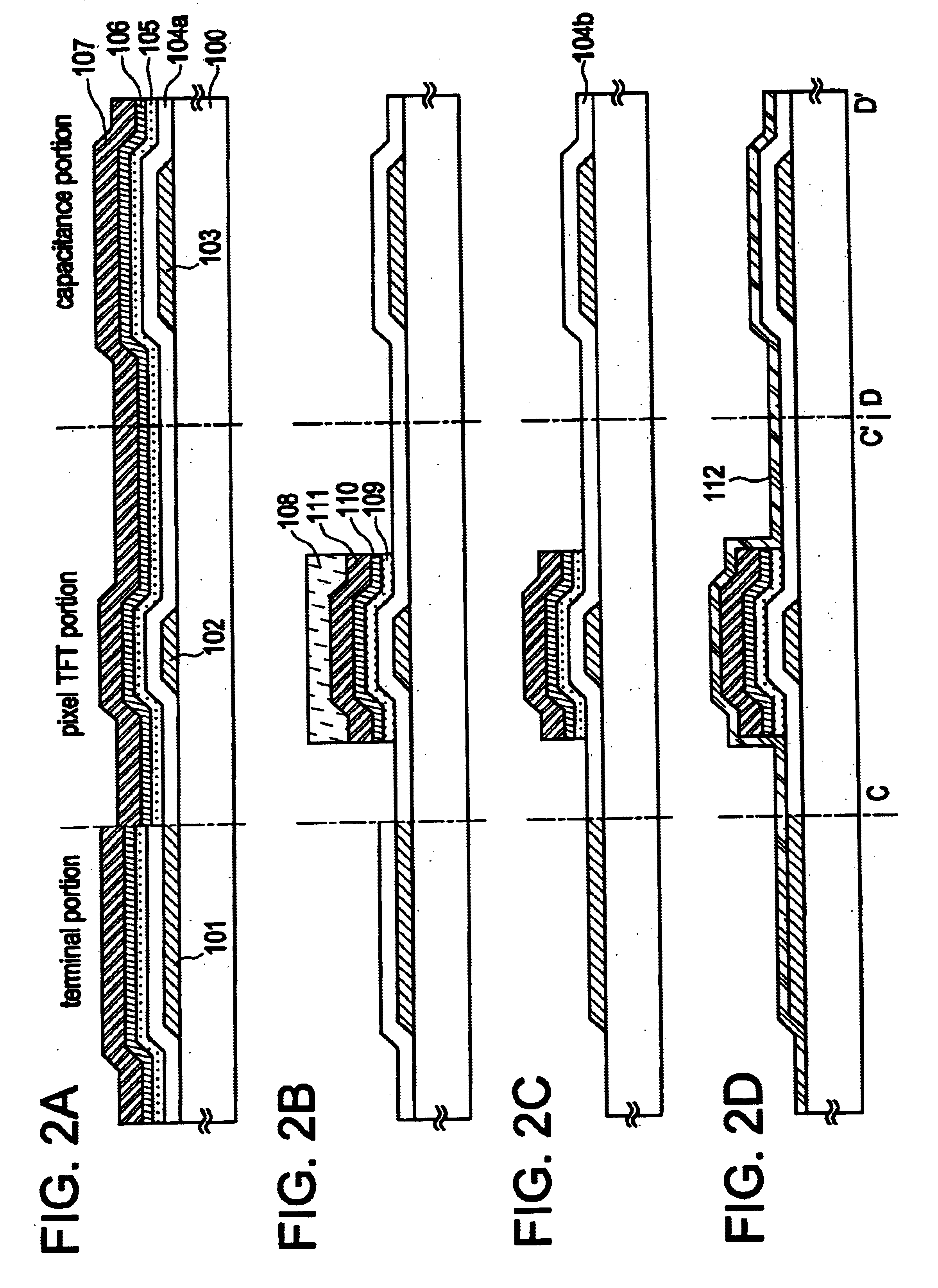
[0107]An embodiment of the invention are explained using FIGS. 1 to 6. Embodiment 1 shows a method of manufacturing a liquid crystal display device, and a detailed explanation of a method of forming a TFT of a pixel portion on a substrate by a reverse stagger type TFT, and manufacturing a storage capacitor connected to the TFT, is made in accordance with the processes used. Further, a manufacturing process for a terminal section, formed in an edge portion of the substrate, and for electrically connecting to wirings of circuits formed on other substrates, is shown at the same time in the same figures.

[0108]In FIG. 2(A), a glass substrate, comprising such as barium borosilicate glass or aluminum borosilicate glass, typically Corning Corp. #7059 or #1737, can be used as a substrate 100 having translucency. In addition, a translucent substrate such as a quartz substrate or a plastic substrate can also be used.

[0109]Next, after forming a conductive layer on the entire surface of the subs...

embodiment 3

[0144]The reverse stagger type n-channel type TFT and the storage capacitor, protected by the inorganic insulating film, can thus be completed in Embodiment 3 by performing the photolithography process using four photomasks four times in total. By thus structuring the pixel portion by arranging these into a matrix state corresponding to each pixel, one substrate for manufacturing the active matrix electro-optical device can be made.

[0145]Note that it is possible to freely combine the constitution of Embodiment 3 with that of Embodiment 1 or Embodiment 2.

[0146]In Embodiment 1 an example centering on forming an insulating film, a first amorphous semiconductor film, a second amorphous semiconductor film, containing an impurity element which imparts n-type conductivity, and a first conductive film by sputtering, but Embodiment 4 shows an example of using plasma CVD to form the films.

[0147]The insulating film, the first amorphous semiconductor film, and the second amorphous semiconductor...

embodiment 4

[0148]In Embodiment 4, a silicon oxynitride film is used as the insulating film, and formed with a thickness of 150 nm by plasma CVD. Plasma CVD may be performed at this point with a power supply frequency of 13 to 70 MHz, preferably between 27 and 60 MHz. By using a power supply frequency of 27 to 60 MHz, a dense insulating film can be formed, and the voltage resistance can be increased as a gate insulating film. Further, a silicon oxynitride film manufactured by adding N2O to SiH4 and NH3 has a reduction in fixed electric charge density, and therefore is a material which is preferable for this use. Of course, the gate insulating film is not limited to this type of silicon oxynitride film, and a single layer or a lamination structure using other insulating films such as s silicon oxide film, a silicon nitride film, or a tantalum oxide film may be formed. Further, a lamination structure of a silicon nitride film in a lower layer, and a silicon oxide film in an upper layer may be use...


PUM


Abstract

A TFT is manufactured using at least five photomasks in a conventional liquid crystal display device, and therefore the manufacturing cost is high. By performing the formation of the pixel electrode, the source region and the drain region by using three photomasks in three photolithography steps, a liquid crystal display device prepared with a pixel TFT portion, having a reverse stagger type n-channel TFT, and a storage capacitor can be realized.

Description

FIELD OF THE INVENTION[0002]The present invention relates to a semiconductor device having a circuit comprised of a thin film transistor (hereafter referred to as TFT), and to a method of manufacturing thereof. For example, the present invention relates to an electro-optical device, typically a liquid crystal display panel, and to electronic appliance loaded with this type of electro-optical device as a part.[0003]Note that, throughout this specification, semiconductor device denotes a general device which can function by utilizing semiconductor characteristics and all of electro-optical devices, semiconductor circuits, and electronic appliances are semiconductor devices.DESCRIPTION OF THE RELATED ART[0004]In recent years, techniques of structuring a thin film transistor (TFT) by using a semiconductor thin film (with a thickness on the order of several nm to several hundred of nm) formed over a substrate having an insulating surface have been in the spotlight. The thin film transist...

Claims


Application Information

Patent Timeline
IPC IPC(8): G02F1/13G02F1/1368H01L21/70H01L27/12H01L21/84G02F1/1362G02F1/136G09F9/30H01L21/336H01L21/77H01L27/13H01L29/786
CPCG02F1/13458H01L27/124H01L27/1255G02F1/1368G02F1/136213H01L2924/181H01L2224/16225H01L2224/32225H01L2224/48091H01L2224/48227H01L2224/48464H01L2224/73204H01L2224/73265H01L2224/45144H01L2924/00014H01L2924/00012H01L2924/00H01L27/12H01L27/1214H01L27/13
Inventor YAMAZAKI, SHUNPEIKOYAMA, JUN
Owner SEMICON ENERGY LAB CO LTD
Why Eureka
Try Eureka