

Method for fabricating a semiconductor device that includes light beam irradiation to separate a semiconductor layer from a single crystal substrate
- Summary
- Abstract
- Description
- Claims
- Application Information
AI Technical Summary
Benefits of technology
Problems solved by technology
Method used
Image

Examples
fifth embodiment
wing respective band structures in a sapphire substrate, a ZnO layer, an AlGaN multilayer portion, and a GaN layer in an epitaxially grown layer ;
[0064]FIG. 13 is a cross-sectional view showing a variation of the fifth embodiment in which an AlGaN multilayer portion is formed to have a multiple quantum well structure;
[0065]FIGS. 14A to 14D are cross-sectional views illustrating a method for fabricating a semiconductor device according to a sixth embodiment of the present invention;
[0066]FIG. 15 is a cross-sectional view showing an exemplary structure of an SiO2 / TiO2 multilayer film according to the sixth embodiment;
[0067]FIGS. 16A to 16D illustrate a conventional method for fabricating a semiconductor device;
[0068]FIG. 17 is a diagram showing a diaphragm in the optical band gap of each of layers in the conventional semiconductor device;
[0069]FIG. 18 is an energy band diagram showing respective band structures in a sapphire substrate, an epitaxially grown layer, and the like accordin...
embodiment 1
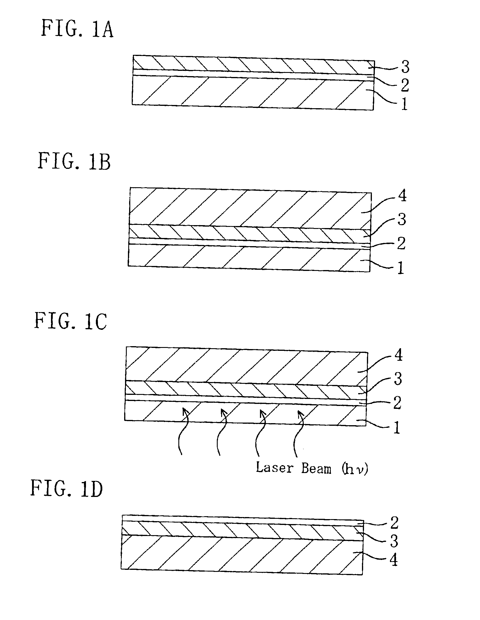
[0072]FIGS. 1A to 1D are cross-sectional views illustrating a method for fabricating a semiconductor device according to a first embodiment of the present invention.
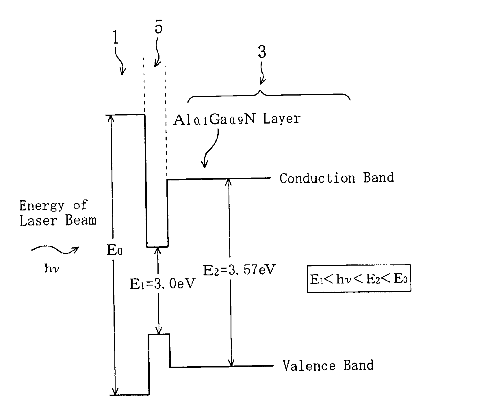
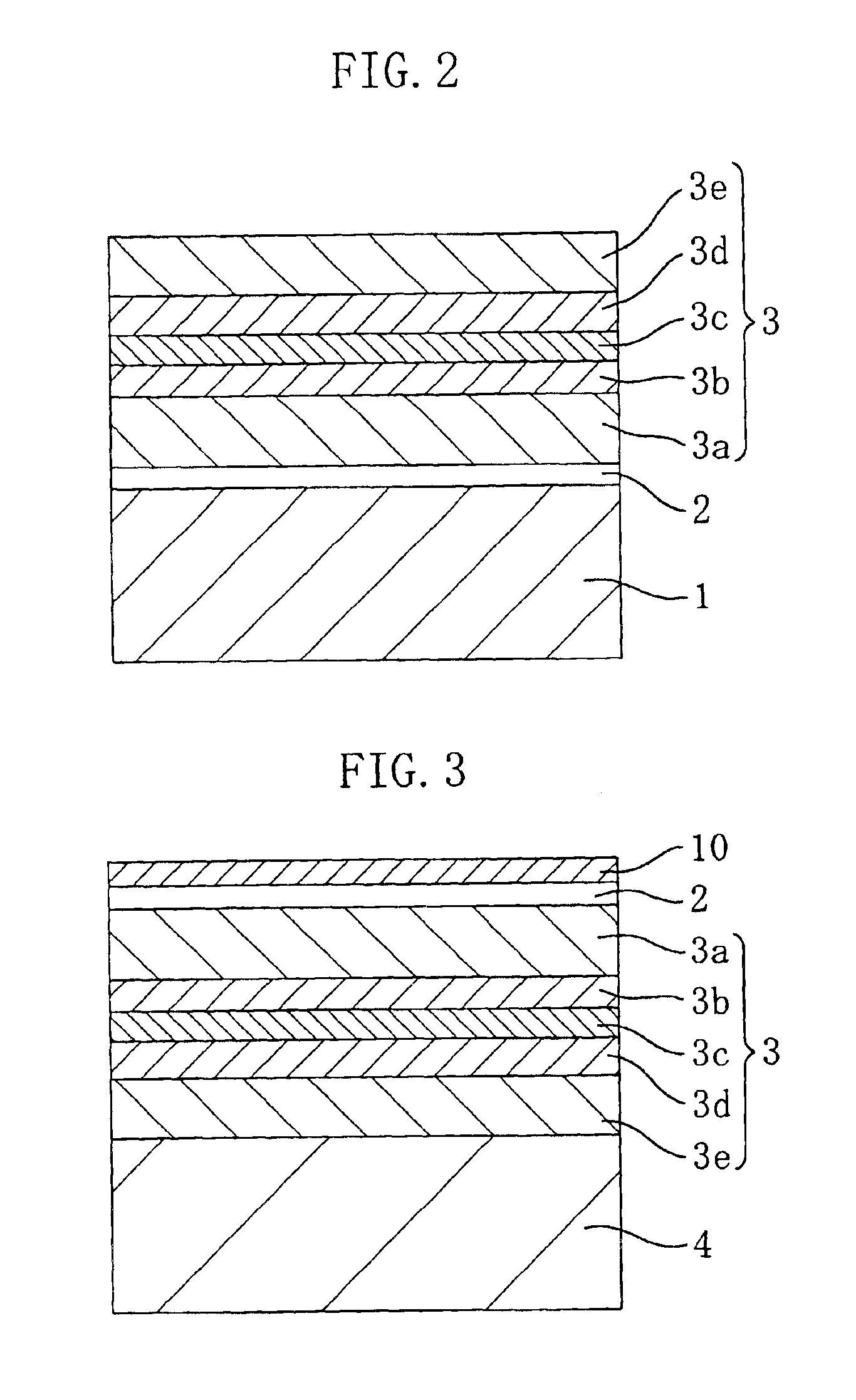
[0073]First, in the step shown in FIG. 1A, a sapphire substrate 1 (wafer) having a principal surface substantially coincident with the (0001) plane (c plane) is prepared. Then, a ZnO layer 2 having a thickness of about 100 nm and serving as a spacer layer is formed by, e.g., RF sputtering on the sapphire substrate 1. Subsequently, an epitaxially grown layer 3 (with a thickness of 5 μm) having a multilayer structure including a GaN layer, an AlGaN layer, and an InGaN layer, each of which is of p-type, of n-type, or undoped, is formed on the ZnO layer 2 by metal organic chemical vapor deposition (MOCVD). In the case of fabricating a semiconductor laser, a waveguide structure has been incorporated into the epitaxially grown layer 3 by using a regrowth technique, selective etching or the like.
[0074]Next, in the step shown in...
embodiment 2
[0084]FIGS. 5A to 5D are cross-sectional views illustrating a method for fabricating a semiconductor device according to a second embodiment of the present invention.
[0085]First, in the step shown in FIG. 5A, a sapphire substrate 1 (wafer) having a principal surface substantially coincident with the (0001) plane (c plane) is prepared. Then, an In0.1Ga0.9N layer 5 having a thickness of about 30 nm and serving as a spacer layer is formed by, e.g., MOCVD on the sapphire substrate 1. Subsequently, an epitaxially grown layer 3 (with a thickness of 5 μm) having a multilayer structure including a GaN layer, an AlGaN layer, and an InGaN layer, each of which is of p-type, of n-type, or undoped, is formed on the In0.1Ga0.9N layer 5 by MOCVD performed in the same apparatus. In the case of fabricating a semiconductor laser, a waveguide structure has been incorporated into the epitaxial layer 3 by using a regrowth technique, selective etching or the like.
[0086]Next, in the step shown in FIG. 5B,...
PUM
 Abstract
Description
Claims
Application Information