

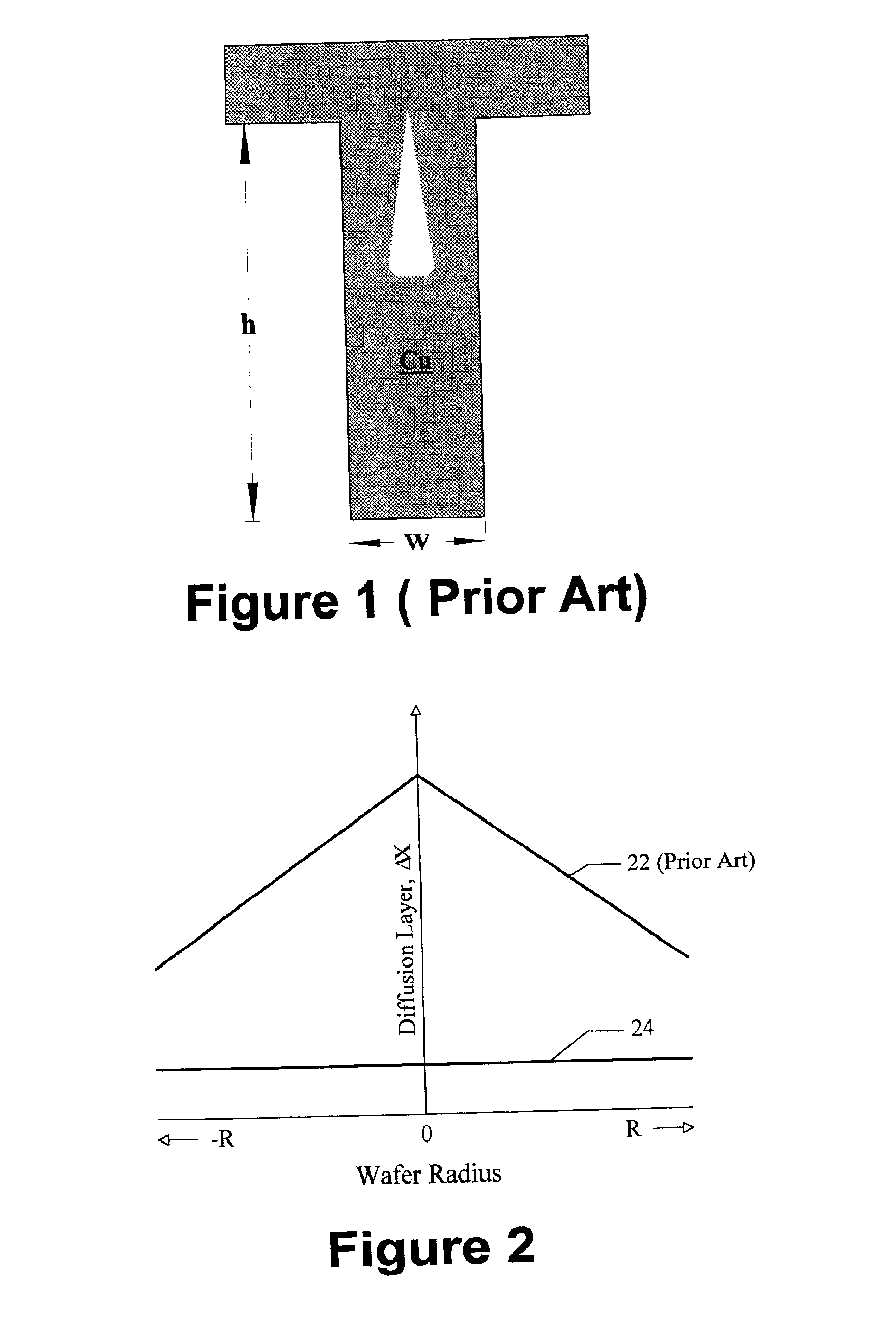
Enhanced electrochemical deposition (ECD) filling of high aspect ratio openings
a technology of electrochemical deposition and high aspect ratio, applied in the direction of electrolysis components, printed element electric connection formation, semiconductor/solid-state device details, etc., can solve the problems of slow plating rate, poor replenishment and depletion of plating ions, and voids in filling, so as to increase inhibition (or suppression) differentiation, enhance the void-free superfilling mechanism, and reduce the plating rate
- Summary
- Abstract
- Description
- Claims
- Application Information
AI Technical Summary
Benefits of technology
Problems solved by technology
Method used
Image

Examples
example 1
Limiting current measurements (of plating current saturation at increasing cathode voltage) were taken with and without jets flow, using a jets ECD (JECD) tool similar to the one disclosed in U.S. Pat. No. 5,421,987. The acidic copper electrolyte did not include any inhibition organic additives. It consisted of 0.3M CuSO4, 10% (v / v) H2SO4, and ˜60 ppm chloride ions. In one measurement, a “natural” flow of about 2 gallons per minute (GPM) was used through an inlet at the bottom of the plating cell. The observed limiting current density, iL, was about 55 mA / cm2. In another measurement, a high pressure of 40 pounds per square inch (PSI) jets flow of 2.8 GPM was used with anode / jets assembly (AJA) rotation speed of 20 RPM, under otherwise identical conditions to the first measurement. The distance between the jet nozzles and the wafer was about 1″. A limiting current iL could not be reached even at current density as high as 733 mA / cm2. Further increase of the cathode voltage merely inc...
example 2
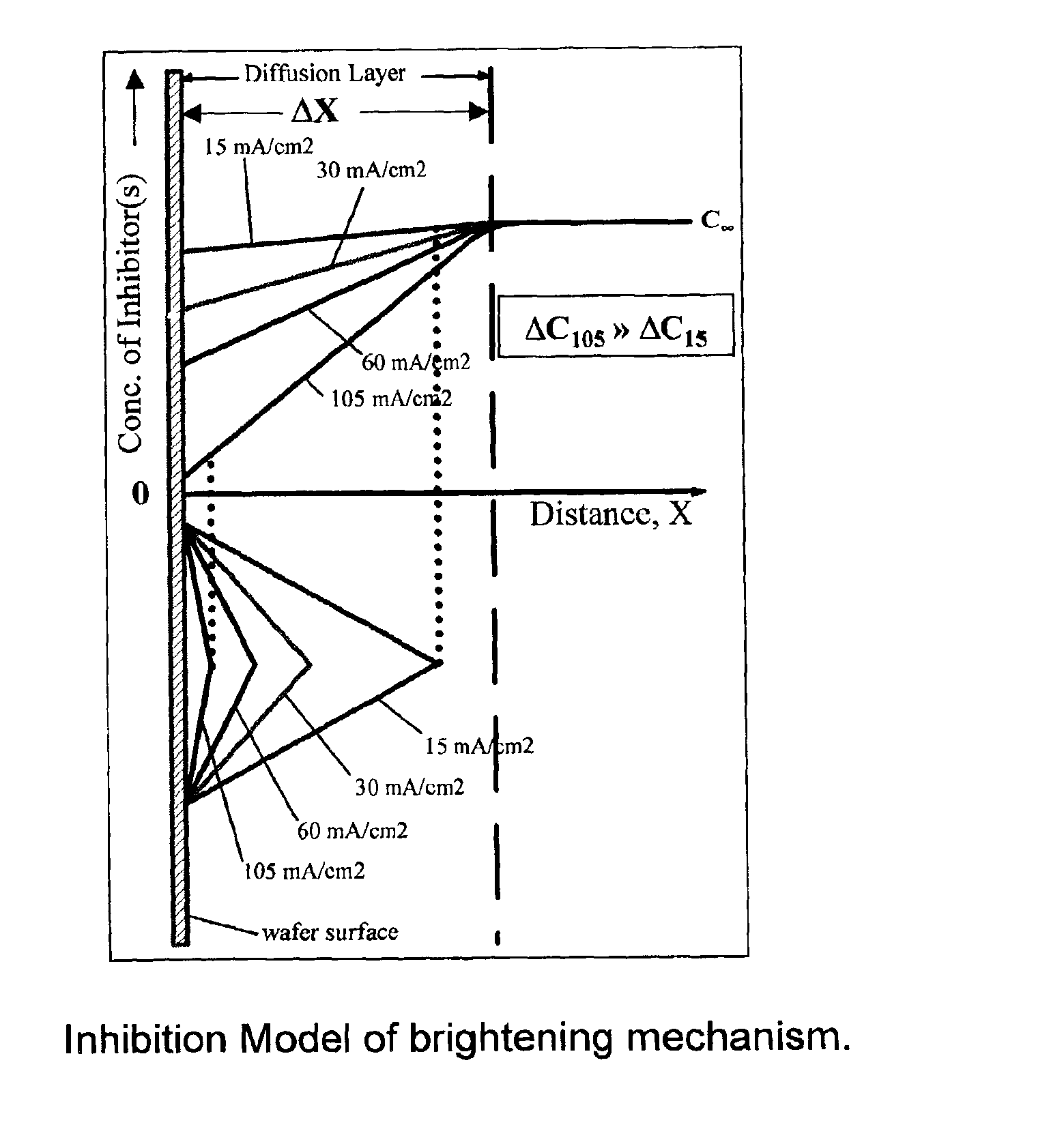
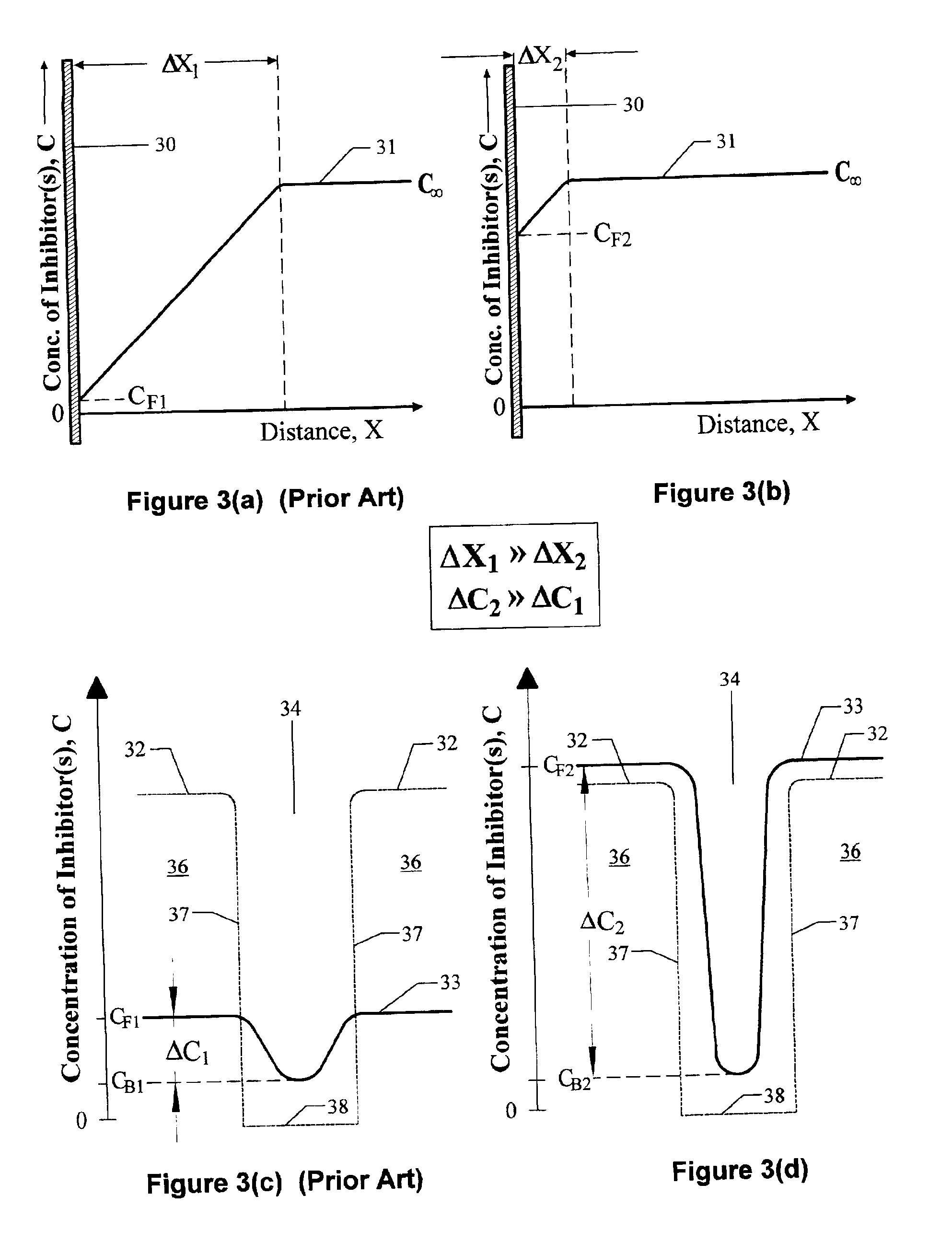
FIG. 4 shows scanning electron micrographs (SEM) of two cleaved samples with Cu-superfilled trenches, in accordance with a preferred embodiment of the invention. Both samples were plated by a jets ECD (JECD) tool, similar to the one disclosed in U.S. Pat. No. 5,421,987. Both samples were plated with current density of 120 mA / cm2 (plating rate of about 2.8 μm / min). FIG. 4(a) shows a sample in which the plating was terminated prior to completion (partially filled trenches), thereby revealing the superfilling profile. The growth profiles on the bottom and sidewalls in FIG. 4(a) correspond well with the superfill model FIG. 3(h). The plating rate is fastest at the bottom (maximum depletion and minimum inhibition) and is slowest at the top (minimum depletion and maximum inhibition) of the openings. It is the plating rate gradients, along the depth of the openings, which facilitate void-free filling of narrow openings. The model and the experimental results imply that, in very narrow open...
example 3
Using a JECD tool as in Example 2, two wafers were plated at low and high plating rates. All other plating parameters (or variables) were identical to those in Example 2. As in FIG. 5, the wafers had patterned arrays of 0.35 / 0.35 μm lines / spaces, and were plated to a nominal thickness of 1.5 μm. The first sample was plated at low current density (15 mA / cm2 or ˜0.35 μm / min), and the second sample was plated at high current density (120 mA / cm2 or ˜2.8 μm / min). While the lower plating rate produced a small step (or hump) of about 140 nm at the field / array border, the sample plated at the higher rate revealed no transition spike or step at all. For comparison, FIG. 5 shows that a wafer plated by a prior art tool had a large spike (˜520 nm) and elevation step (˜250 nm) at the border. Surface roughness of JECD plated samples was measured by AFM. While the mean surface roughness (Ra) of a low current (15 mA / cm2) sample was 11.2 nm, that of a sample plated at the higher current (120 mA / cm2)...
PUM
| Property | Measurement | Unit |
|---|---|---|
| current density | aaaaa | aaaaa |
| current density | aaaaa | aaaaa |
| current density | aaaaa | aaaaa |
Abstract
Description
Claims
Application Information