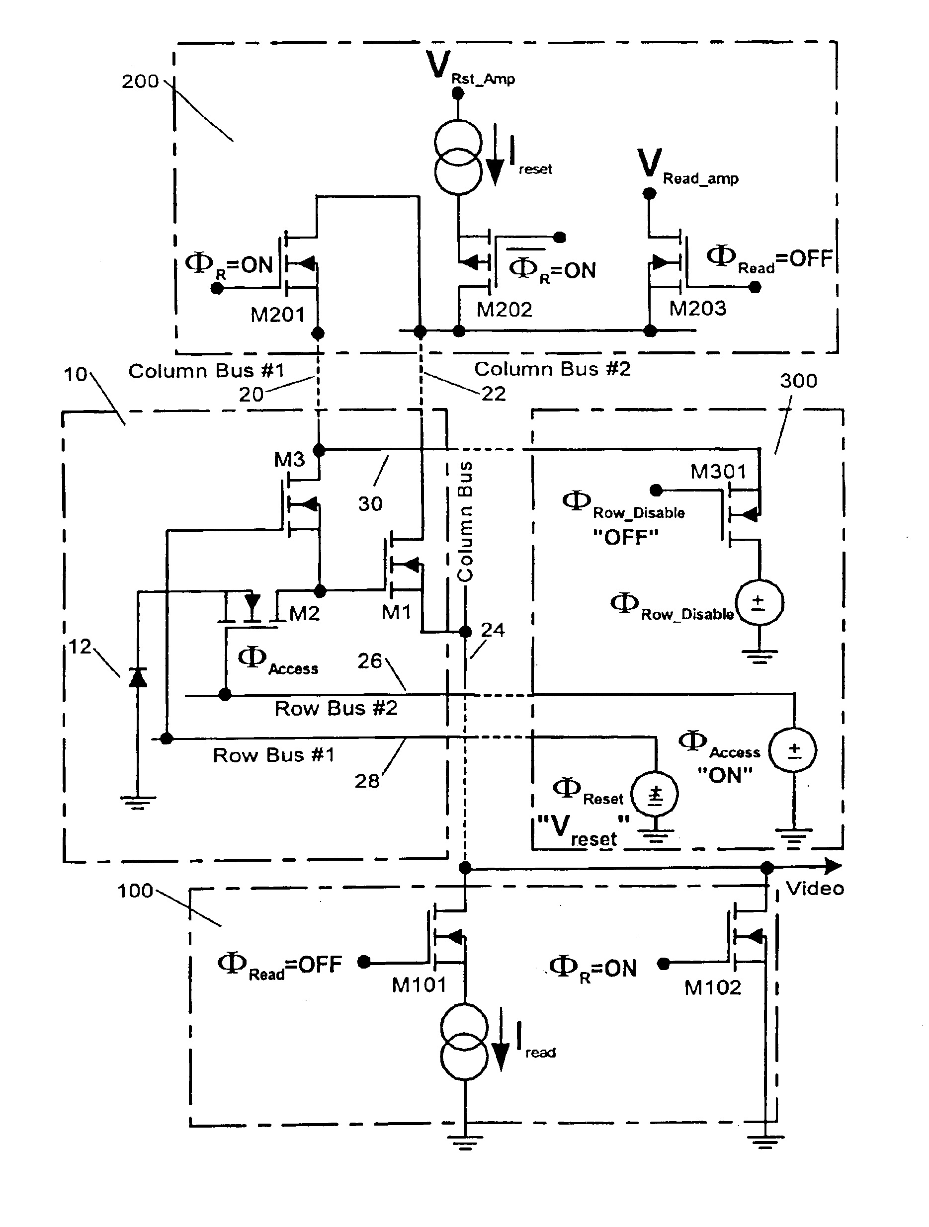
[0010]In general, the present invention comprises a low-noise imaging
system for implementation in CMOS or in other
semiconductor fabrication technologies. The low-noise
amplifier system efficiently suppresses reset (kTC) noise by using a compact
preamplifier consisting of a
photodetector and only three transistors of identical polarity in conjunction with ancillary circuits located on the CMOS imager's periphery. A tapered reset signal is applied to a reset
transistor within the pixel to reduce the reset noise. The supporting circuits help the simplified pixel circuit to read the signal with
low noise without having to perform
correlated double sampling on either successive rows or the entire array.
[0011]The
low noise amplifier system of the present invention is formed by the aggregate circuitry in each pixel, the supporting circuitry in the column
buffer amplifier and the row-based
clock driver, and the waveform generation circuits servicing each column and row of pixels. The video from the active pixels is read out by the low-noise
signal amplification system in a manner that essentially eliminates the reset noise. In addition to means for suppressing the
detector's reset noise, the column buffer in the downstream
electronics typically performs additional
signal processing, sample-and-hold, optional video pipelining, and column
amplifier offset cancellation functions to suppress the temporal and
spatial noise that could otherwise be generated by the column buffer.
[0012]The low-noise system provides the following key functions: (1) suppresses reset noise without having to provide means for
analog memory to facilitate
correlated double sampling; (2) provides high sensitivity via source follower amplification with small sense
capacitance; (3) minimizes demand on amplifier bandwidth to avoid generation of
fixed pattern noise due to variations in amplifier
time constant and stray
capacitance; (4) provides adequate power supply rejection to enable development of imaging systems-on-a-
chip that do not require elaborate support
electronics; and (5) is compatible with application to imaging arrays having pixel
pitch to below 2.7 microns with high optical
fill factor and low noise using 0.18 μm CMOS technology.
[0013]The invention has the
advantage of full process compatibility with standard silicided submicron CMOS; helps to maximize yield and minimize die cost because the
circuit complexity is distributed amongst the active-pixels and
peripheral circuits; and exploits the
signal processing capability inherent to CMOS. Also, the
spectral response is broad from the near-
ultraviolet (400 nm) to the near-IR (>800 nm).
[0014]Because the present invention has only three MOSFETs in each pixel, the invention provides as-drawn optical
fill factor of 60% at 5 μm pixel
pitch using 0.25 μm design rules in CMOS. The actual optical
fill factor is somewhat larger due to lateral collection and the large
diffusion length of commercial CMOS processes. A final
advantage is the flexibility to collocate digital logic and signal-
processing circuits due its high
immunity to
electromagnetic interference.
[0015]When fully implemented in the desired camera-on-a-
chip architecture, the low-noise APS can provide temporal read noise below 10 e− (at data rates compatible with either
video imaging or still photography via electronic means),
fixed pattern noise significantly below 0.02% of the maximum signal (on a par with competing CCD imagers), <0.5% nonlinearity, >1V signal swing for 3.3 V power supply, large charge-handling capacity, and variable sensitivity using simple serial interface updated on a frame-by-frame basis via
digital interface to a host
microprocessor.


