Semiconductor device, liquid crystal display device, EL display device, method for fabricating semiconductor thin film, and method for manufacturing the semiconductor device

a semiconductor and liquid crystal display technology, applied in the field of semiconductor devices, can solve the problems of deterioration of response capability and the like, impairment of reliability, and irregular performance in the production of tft, and achieve the effect of large siz

Inactive Publication Date: 2005-06-14
JOLED INC
View PDF14 Cites 48 Cited by
  • Summary
  • Abstract
  • Description
  • Claims
  • Application Information

AI Technical Summary

Benefits of technology

[0009]A main object of the present invention is to provide a polycrystalline semiconductor thin film having a crystal of large size.

Problems solved by technology

(1) The crystals in a polycrystalline silicon thin film thus formed have a small size so that due to low mobility of electron, response capability and the like are deteriorated in producing a TFT.
(2) In a TFT, numerous grain boundaries of silicon crystals may be present in a boundary between a lightly doped drain area (hereinafter referred to as “LDD area”) or an offset area and a channel area or in its vicinity. In this case, a large number of crystalline defects and dangling bonds exist in the vicinity of the grain boundary so that the performance is deteriorated when the TFT Is allowed to execute a switching operation continuously for a long time or repeatedly many times, resulting in impairment of reliability.
(3) In producing a TFT or a display device, no means is available for determining the positional relationship between the crystals of silicon thin film and TFT pattern, so that it is impossible to determine the position of grain boundary of silicon crystal with respect to the TFT. This results in irregularities of performance in producing a TFT.

Method used


Image

  • Semiconductor device, liquid crystal display device, EL display device, method for fabricating semiconductor thin film, and method for manufacturing the semiconductor device
  • Semiconductor device, liquid crystal display device, EL display device, method for fabricating semiconductor thin film, and method for manufacturing the semiconductor device
  • Semiconductor device, liquid crystal display device, EL display device, method for fabricating semiconductor thin film, and method for manufacturing the semiconductor device

Examples


embodiment 1

(Embodiment 1)

(Semiconductor thin film)

[0127]First, a method of producing a semiconductor thin film will be described. The producing methods in this embodiment and in the other embodiments can be carried out in the same manner relating to semiconductor thin films made of, e.g., GaAs, Ge, SiGe, SiGeC or the like. Nevertheless, the methods will be discussed mainly relating to silicon (Si) generally used these days.

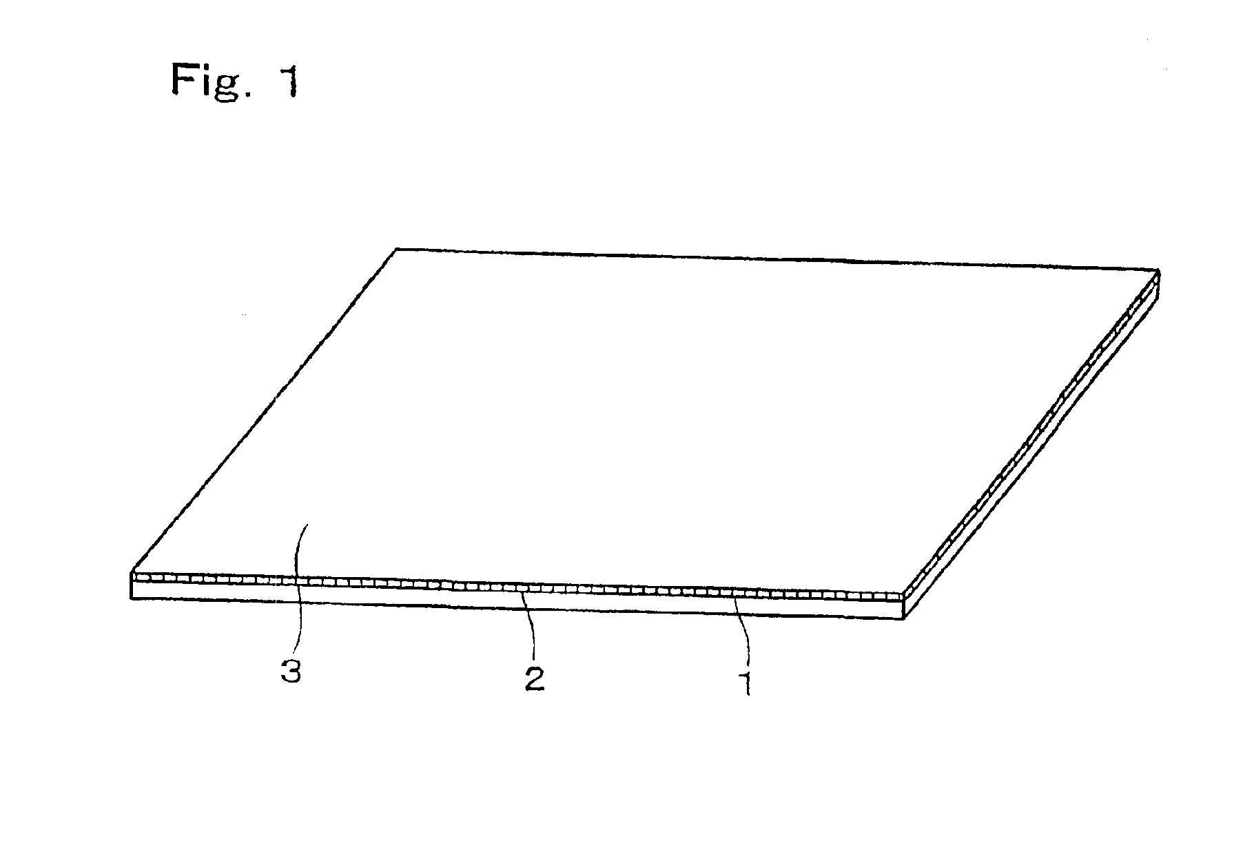
[0128]As shown in FIG. 1, an undercoat film 2 formed of SiO2 having a thickness of 300 nm is formed on a substrate 1, e.g., by a TEOS-CVD method in order to prevent diffusion of dopants from the substrate 1. The thickness of the undercoat film 2 is not limited to 300 nm but can be set in a broad range. The substrate 1 is made of glass in this embodiment, and may be composed of plastics or may be films. Silicon nitride films or the like can be used as the undercoat film 2. No problem would be posed if a SiO2 film or silicon nitride film has a thickness of 200 nm or more. The ...

embodiment 2

(Embodiment 2)

[0165]An embodiment 2 of the invention will be described. Constituent parts having the same function in this embodiment and in the following embodiments as those described above in the embodiment 1 are indicated by the same reference numerals in the drawings. The description of this embodiment on the matters already stated in respect of the embodiment 1 will be omitted.

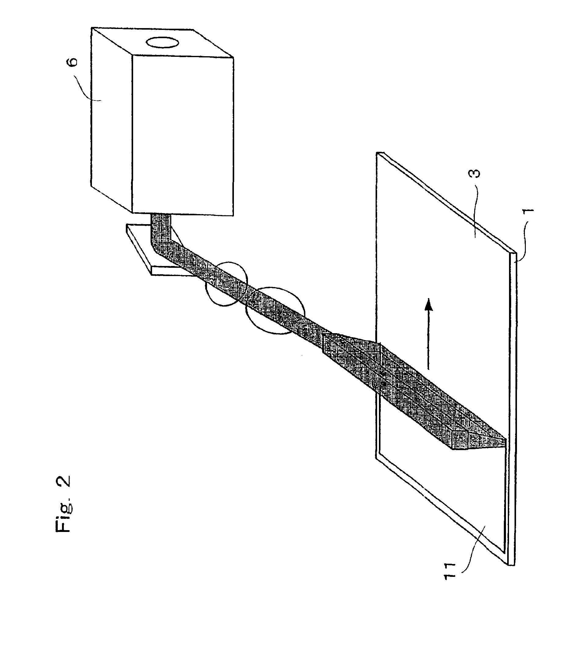
[0166]A method of producing a semiconductor thin film in the embodiment 2 is characterized in that in the method of producing a semiconductor thin film in the embodiment 1, laser light beams 7 in the primary irradiation step is applied at a frequency which is different from that involved in the embodiment 1. More specifically, laser beams 7 are repeatedly applied to a specified range of region on the substrate a plurality of times in the embodiment 1, whereas laser beams are modulated so as to accomplish irradiation to the entire surface of the substrate at one time (one pulse) and is applied to the spec...

embodiment 3

(Embodiment 3)

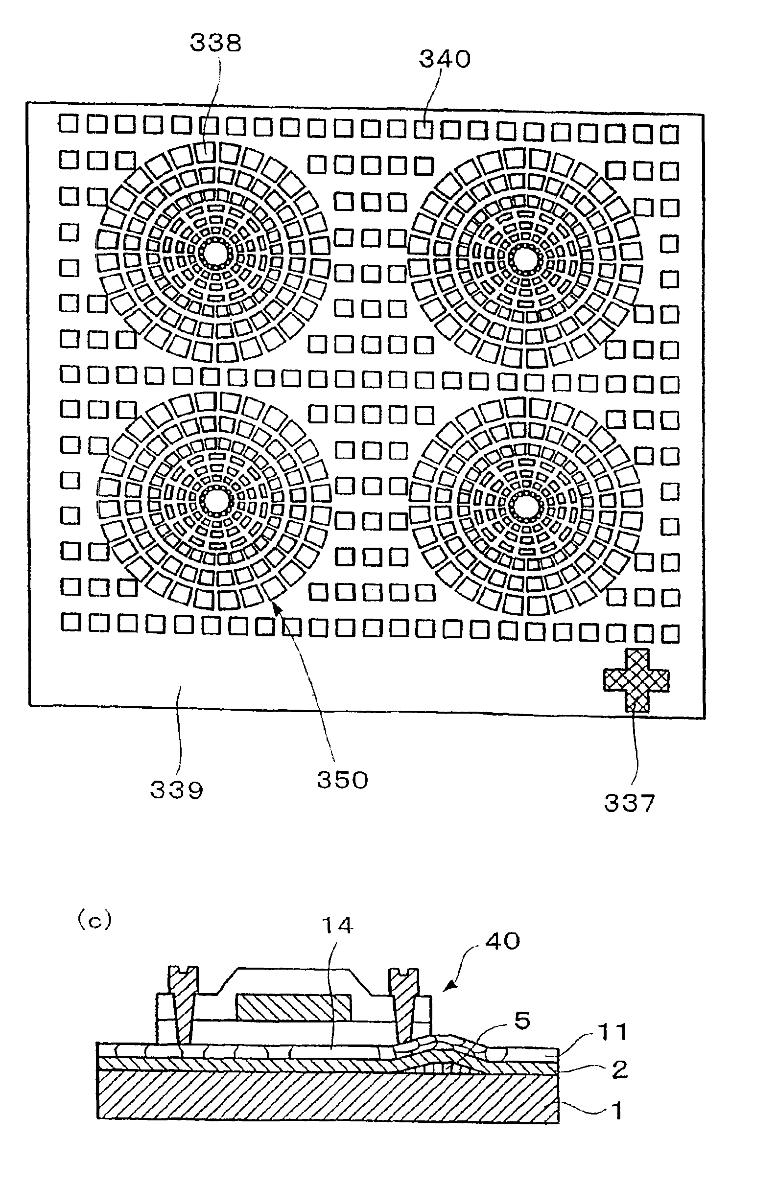
[0170]An embodiment 3 of the invention will be described. A method of producing a semiconductor thin film according to the embodiment 3 is different from the method of the embodiment 1 in that in the embodiment 3, the step of forming a heat-dissipating layer 4 and an alignment key 5 is carried out without executing the pre-irradiation step, and this step is done by liftoff.

[0171]More specifically, a resist pattern R is formed by applying a resist to the dehydrogenated amorphous silicon film 3 by photolithography to cover other portions than portions corresponding to the heat-dissipating layer 4 and the alignment key 5 (FIG. 16(a)). An MoW film M is formed by vapor deposition (FIG. 16(b)). Then the heat-dissipating layer 4 and the alignment key 5 are formed by removing the resist pattern R and the MoW film M on the resist pattern R by a resist release agent to form the heat-dissipating layer 4 and the alignment key 5 (FIG. 16(c)).

[0172]Next, the primary irradiation step...


PUM

PropertyMeasurementUnit
diameteraaaaaaaaaa
gate voltageaaaaaaaaaa
frequencyaaaaaaaaaa

Abstract

This invention concerns with a semiconductor device which is characterized in that the device is provided with a thin film transistor 40 having a polycrystalline semiconductor layer 11, the semiconductor layer 11 including a channel area 22, highly doped drain areas 24, 17 positioned on both sides of the channel area 22 and LDD areas 18a, 18b positioned between the channel area 22 and the highly doped drain areas 24, 17 and lower in dopant density than the highly doped drain areas 24, 17, wherein any diameter of the crystal 14 at least partly existing in the LDD area 18b is larger than the size of other crystals 15.

Description

FIELD OF THE INVENTION[0001]The present invention relates to a semiconductor device, a liquid crystal display device, an EL display device, a method for fabricating a semiconductor thin film and a method for manufacturing the semiconductor device.BACKGROUND ART[0002]A laser anneal method is generally known as a method of producing a semiconductor thin film for forming a semiconductor layer of a thin film transistor (hereinafter referred to as “TFT”). The laser anneal method comprises the steps of forming an amorphous semiconductor film or a microcrystalline semiconductor film on a substrate made of glass or the like, and irradiating the film with laser beams for crystallization to give a polycrystalline semiconductor film. Usually this method is called a crystallization process.[0003]Argon laser, KrF and XeCl excimer laser are generally used as a light source for laser beams to be employed in the crystallization process. The TFT produced by the foregoing method is generally called a...

Claims


Application Information

Patent Timeline
Patent Type & Authority Patents(United States)
IPC IPC(8): H01L21/336H01L29/786H01L21/02H01L21/20H01L21/70H01L29/66H01L21/84H01L27/12G02F1/13G02F1/1368H01L21/77H01L29/04
CPCH01L21/2026H01L27/12H01L29/04H01L29/66757H01L27/1281H01L29/78603H01L29/78621H01L29/78675H01L29/78678H01L29/66765G02F1/1368H01L21/02683H01L21/02686H01L21/02422H01L21/02488H01L21/02678H01L21/02532H01L21/02595H01L21/02691
Inventor NISHITANI, HIKARUYAMAMOTO, MAKOTOTAKETOMI, YOSHINAO
Owner JOLED INC
Why Eureka
Try Eureka