Organic luminescence device

a luminescence device and organic technology, applied in the direction of discharge tube/lamp details, group 3/13 element organic compounds, natural mineral layered products, etc., can solve the problems of insufficient durability affecting the efficiency of the luminescence device, etc., to achieve easy production and relatively inexpensive effects

Inactive Publication Date: 2005-07-12
CANON KK
View PDF37 Cites 21 Cited by
  • Summary
  • Abstract
  • Description
  • Claims
  • Application Information

AI Technical Summary

Benefits of technology

[0011]A more specific object of the present invention is to provide an organic (electro-) luminescence device capable of effecting light output (emission) at high efficiency and luminance while realizing a prolonged life.
[0012]Another object of the present invention is to provide an organic luminescence device capable of providing a wide variety of emission wavelengths and emission hues, inclusive of particularly orange and red hues, and a good durability.
[0013]A further object of the present invention is to provide an organic luminescence device which can be produced easily and relatively inexpensively.

Problems solved by technology

These organic luminescence devices are also still insufficient in terms of durability such that the devices are liable to be changed in their properties with time when used for a long period or liable to be deteriorated by the influence of ambient air containing oxygen or of humidity.
However, a satisfactory solution to the problem has not been realized yet, and particularly a red luminescence with a good color purity has not been satisfactorily provided.
A proposal of using a spiro compound in an organic luminescence device has been reported (JP-A 7-278537) but has failed to provide an electron-transporting layer or a luminescence layer exhibiting sufficient luminescence performance.

Method used


Image

  • Organic luminescence device
  • Organic luminescence device
  • Organic luminescence device

Examples


example a-1

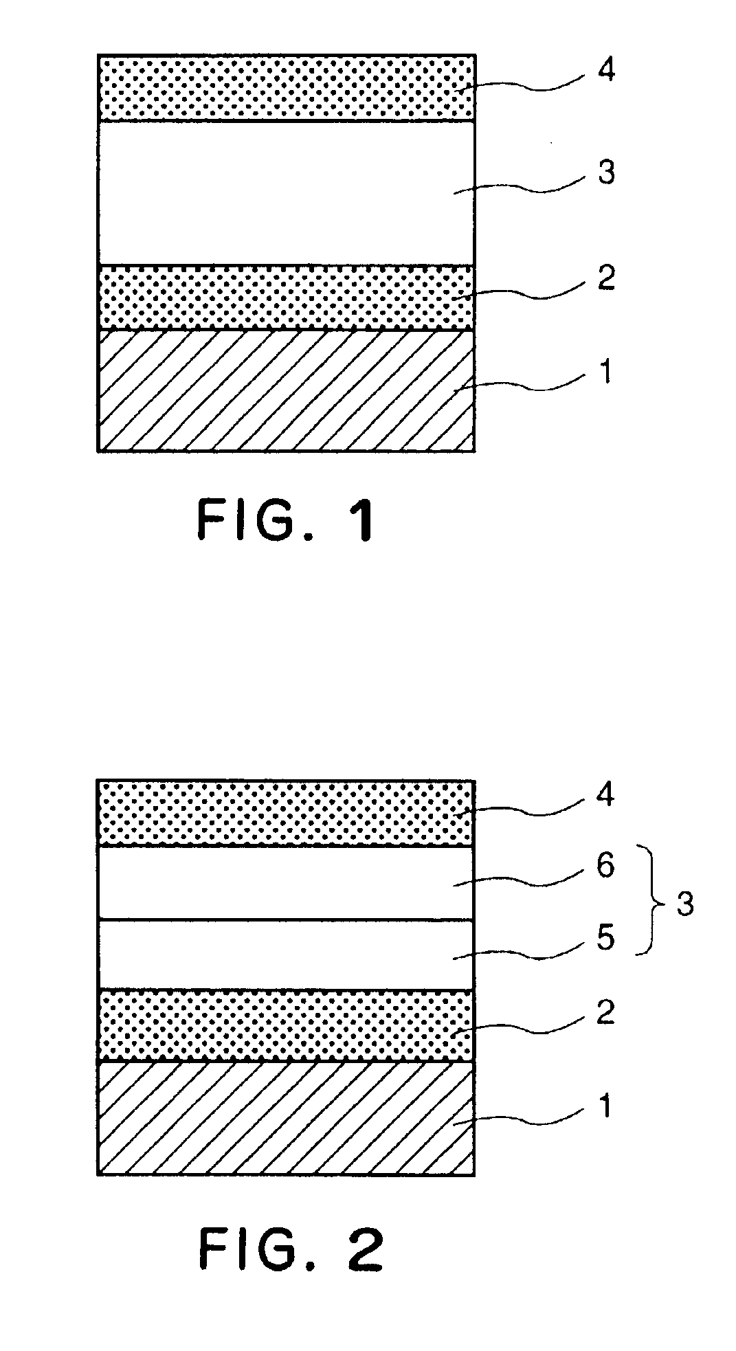
[0077]An electroluminescence device of a structure as shown in FIG. 2 was prepared in the following manner.

[0078]A 0.7 mm-thick glass substrate (substrate 1) coated with a 120 nm-thick film of ITO (indium tin oxide) (anode 2) formed by sputtering was successively washed with acetone and isopropyl alcohol (IPA) under application of ultrasonic wave and then washed with IPA under boiling, followed by cleaning by UV / ozone (i.e., irradiation with ultraviolet rays in the ozone-containing atmosphere), to obtain a transparent conductive substrate (including the substrate 1 and the ITO anode 2 formed thereon).

[0079]The transparent conductive substrate was coated by vacuum deposition of a compound (TPD) represented by a structural formula shown below:

to form a 70 nm-thick hole-transporting layer 5 and then by vacuum deposition of a spiro compound (Example Compound No. a-1 listed in Table 1) to form a 70 nm-thick electron-transporting layer 6. The vacuum deposition was respectively performed ...

examples a-2

to A-20

[0083]Organic luminescence devices were prepared and evaluated in the same manner as in Example A-1 except for replacing the Spiro compound (Ex. Comp. No. a-1) with those shown in Table 17, respectively.

[0084]The results are inclusively shown in Table 17 set forth hereinafter.

example a-21

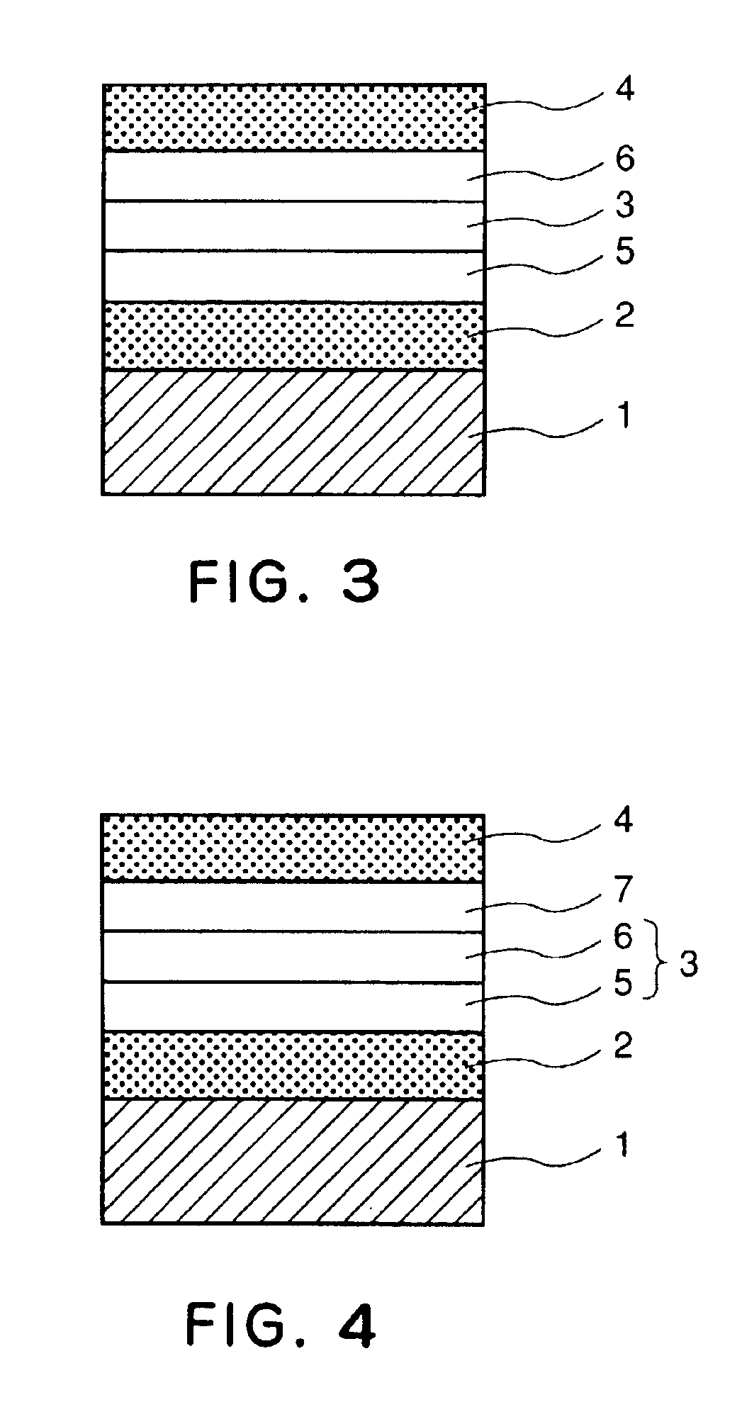
[0087]The procedure of Example A-1 was repeated up to the formation of the hole-transporting layer 5.

[0088]Then, the hole-transporting layer 5 was further coated by vacuum deposition of a mixture of spiro compound (Ex. Compound No. a-2) and aluminum tris(quinolinol) in a weight ratio of 1:20 to form a 70 nm-thick electron-transporting layer 6 under a vacuum of 1.0×10⁻⁴ Pa and at a film thickness growth rate of 0.2-0.3 nm / sec.

[0089]Then, the electron-transporting layer 6 was further coated by vacuum deposition of Al—Li alloy (Li content: 1 atom. %) to form a 150 nm-thick metal film 4 under a vacuum of 1.0×10⁻⁴ Pa and at a film thickness growth rate of 1.0-1.2 nm / sec, thereby forming an organic luminescence device of a structure shown in FIG. 2.

[0090]The thus-obtained device was then supplied with a DC voltage of 8 volts between the ITO electrode 2 as an anode and the Al—Li alloy electrode 4 as a cathode, whereby a current flowed at a density of 9.0 mA / cm2 and orange luminescence was ...


PUM

PropertyMeasurementUnit
thicknessaaaaaaaaaa
thicknessaaaaaaaaaa
thicknessaaaaaaaaaa

Abstract

In an organic luminescence device formed of one or plural layers of organic films between an anode and a cathode, at least one layer is any one of a luminescence layer, an electron injection layer and an electron-transporting layer and is formed of at least a spiro compound of formula (I-a) or (I-b) having a carbon atom or a silicon atom as a spiro atom and having four ring structures including at least one nitrogen atom-containing ring structure. By the use of the spiro compound of the formula (I-a) or (I-b), the resultant organic luminescence device produces a high-luminance fluorescent luminescence at a low voltage for a long period of time.

Description

[0001]This is a continuation of PCT / JP 02 / 08803, filed Aug. 30, 2002.TECHNICAL FIELD[0002]The present invention relates to an organic (electro-)luminescence device and particularly to an organic luminescence device for emitting light by applying an electric field to a film of an organic compound (organic compound layer).BACKGROUND ART[0003]An organic luminescence device generally comprises a pair of electrodes (comprising an anode and a cathode) and a film comprising a fluorescent organic compound disposed between the electrodes. Into the organic compound layer (film), holes and electrons are injected from the anode and the cathode, respectively, thus forming excitons of the fluorescent organic compound. When the excitons are returned to ground state, the organic luminescence device emits light or causes luminescence.[0004]According to a study by Eastman Kodak Co. (“Appl. Phys. Lett.”, vol. 51, pp. 913- (1987)), it has been reported that a function-separation type organic luminescen...

Claims


Application Information

Patent Timeline
Patent Type & Authority Patents(United States)
IPC IPC(8): C08G61/12C08G61/00C08G61/02C09K11/06H01L51/05H01L51/30H05B33/14H01L51/50H01L51/00
CPCC08G61/02C08G61/12C08G61/123C09K11/06H01L51/0058H01L51/0069H01L51/0071H01L51/0094H05B33/14H01L51/0034H01L51/0035H01L51/0036H01L51/0038H01L51/0039H01L51/004H01L51/0042H01L51/0043H01L51/005H01L51/0052H01L51/0053H01L51/0059H01L51/007H01L51/0077H01L51/0078H01L51/0081H01L51/5012H01L51/5048H01L51/5092Y10S428/917H10K85/10H10K85/111H10K85/113H10K85/115H10K85/146H10K85/141H10K85/114H10K85/151H10K85/60H10K85/621H10K85/615H10K85/631H10K85/626H10K85/656H10K85/6565H10K85/657H10K85/311H10K85/30H10K85/324H10K85/40H10K50/11H10K50/14H10K50/171
Inventor SUZUKI, KOICHISENOO, AKIHIROUENO, KAZUNORI
Owner CANON KK
Why Eureka
Try Eureka