Method of forming an oxide film

a technology of oxide film and gate insulating film, which is applied in the direction of vacuum evaporation coating, solid-state devices, coatings, etc., can solve the problems of interfacial level formation, fixed electric charge generation in gate insulating film, and give damage thereto, so as to achieve high reliability, high performance, and high performance.

Inactive Publication Date: 2005-11-01
SEMICON ENERGY LAB CO LTD
View PDF42 Cites 357 Cited by
  • Summary
  • Abstract
  • Description
  • Claims
  • Application Information

AI Technical Summary

Benefits of technology

[0020]It is another object of the present invention to provide a method of manufacturing a thin film transistor of high performance at a low temperature.
[0037]As the oxidizing gas used in the present invention, oxygen, ozone, dinitrogen monoxide (nitrous oxide), and the like are preferable. In the case of ozone or oxygen, oxygen atoms in the ozone or oxygen might be involved in an obtained oxide film, however, the oxygen atoms do not cause fixed electric charges in the obtained film since they are main ingredients of the oxide film. Accordingly an extremely fine oxide film involving less impurity atoms can be obtained. Besides, since the mass of the oxygen atom is less than that of an Ar atom, even if such oxygen atoms collide with an oxide film formed on a substrate during the film formation, there are few defects caused in the oxide film. Therefore, an excellent oxide film can be obtained.

Problems solved by technology

However, in both the plasma CVD and the sputtering method using a large amount of argon, the gate insulating film involves numbers of elements (e.g. inert gas elements such as Ar) which was involved in a target or existed in a chamber during the CVD or the sputtering, resulting in generation of fixed electric charges in the gate insulating film.
Further, ions of the elements bombard a surface of an activated layer in a thin film transistor and thereby give a damage thereto.
As a result, interfacial level is formed at the interface and a thin film transistor of fine characteristics cannot be obtained by any of those methods.
However, the photo CVD method required a long period of time, in other words, the film formation speed was extremely slow, so that the photo CVD method was not suitable for an industrial application.
This is partly because internal stress is generated in the silicon oxide film by Ar or Ar+ present inside the silicon oxide network and partly because defects are formed in the silicon oxide film by bombardment of argon with the silicon oxide film during sputtering.

Method used


Image

  • Method of forming an oxide film
  • Method of forming an oxide film
  • Method of forming an oxide film

Examples


embodiment no.1

(Embodiment No. 1)

[0050]Referring to FIG. 6(A), a planar type magnetron RF sputtering apparatus suitable for use in manufacturing oxide films or electronic devices in accordance with the present invention is illustrated. The apparatus comprises a vacuum chamber 31, an evacuation system 32 consisting of a turbo molecular pump 32b and a rotary pump 32d respectively provided with valves 32a and 32c, a metallic holder 33 fixed in the lower side of the chamber 31 for supporting a target 34 thereon, formed with an inner conduit 33a through which a coolant can flow to cool the target 34 and provided with a number of permanent magnets 33b, an energy supply 35 consisting of an RF (e.g. 13.56 MHz) source 35a provided with a matching box 35b for supplying RF energy to the holder 33, a substrate holder 36 located in the upper position of the chamber 31 for supporting a substrate 1 to be coated, a heater 36a embedded in the substrate holder 36, a shutter 37 intervening the substrate 1 and the ta...

embodiment no.2

(Embodiment No. 2)

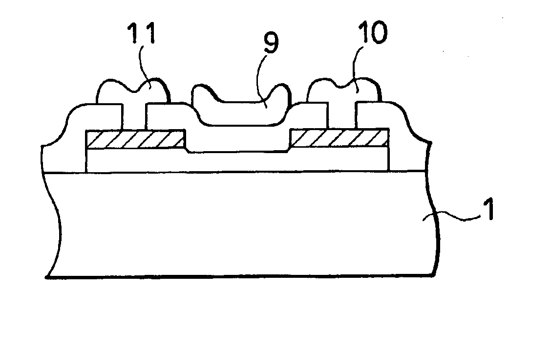
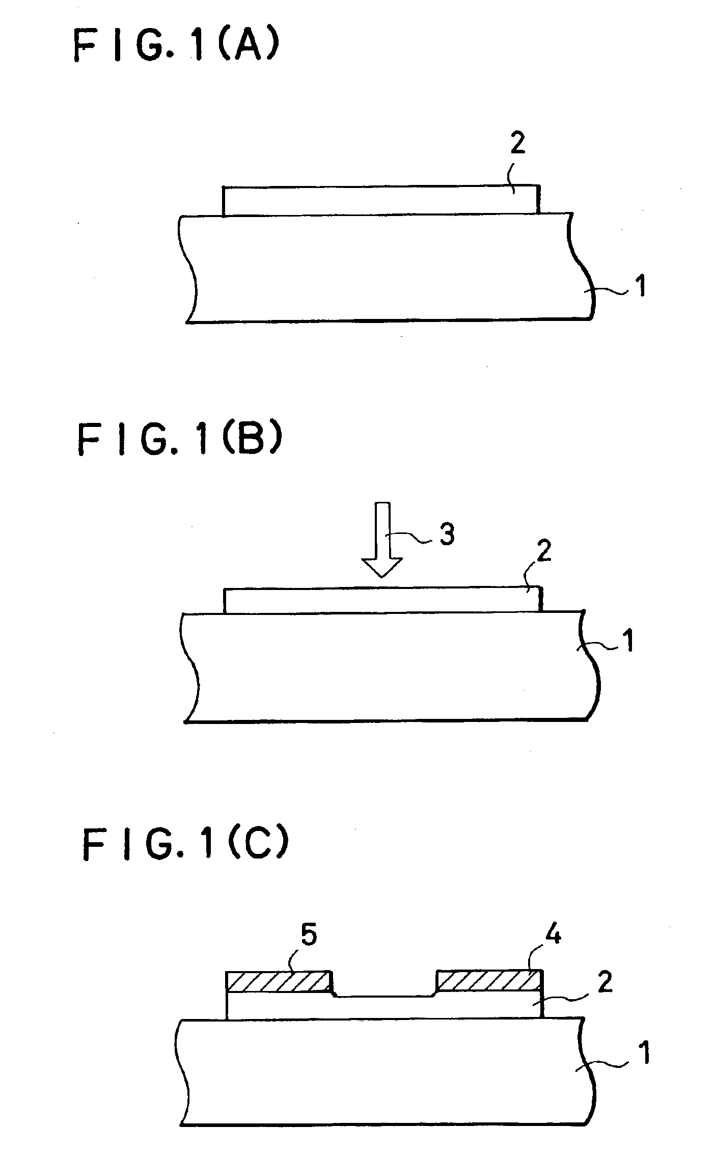
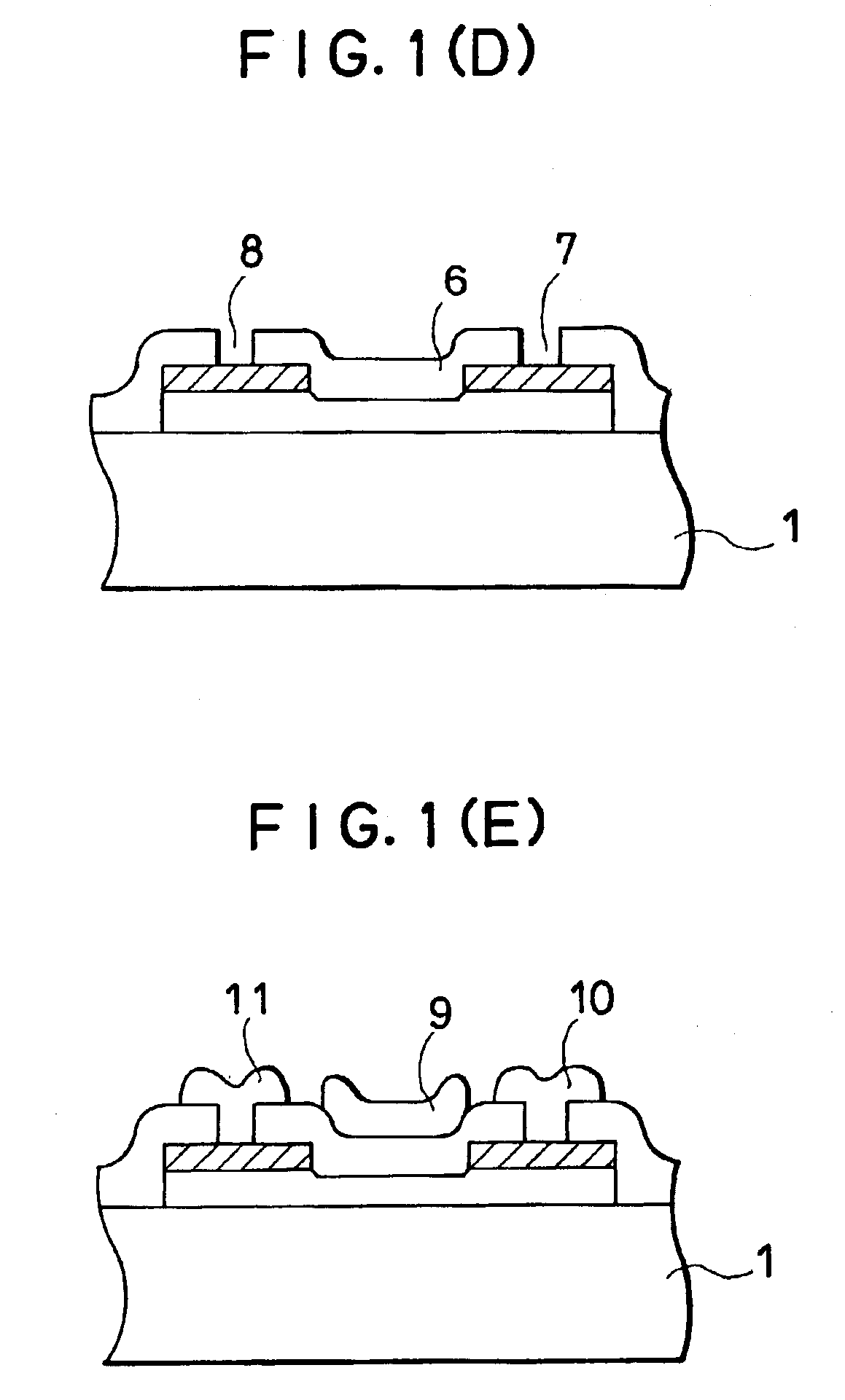
[0075]Referring to FIGS. 1(A) to (E), manufacturing steps of a thin film transistor in accordance with this embodiment are illustrated.

[0076]In this embodiment, a soda-lime glass having a blocking layer such as silicon oxide or silicon nitride provided thereon was used as a substrate 1. On the substrate 1, an I-type non-single crystalline semiconductor layer was formed by a known plasma CVD. Followings are conditions of the formation of the above semiconductor layer.

[0077]

Substrate Temperature350°C.Pressure during Reaction0.06TorrRF Power (13.56 MHz)100WGas to be UsedSiH4Film Thickness2000Å

[0078]The semiconductor layer was patterned into semiconductor islands with a metal mask.

[0079]The patterning may be carried out by means of a known photolithography technique instead of the metal mask. In FIGS. 1(A) to (E), reference numeral 2 designates one of the semiconductor islands.

[0080]Then, as shown in FIG. 1(B), the non-single crystalline semiconductor island 2 was crys...


PUM

PropertyMeasurementUnit
temperatureaaaaaaaaaa

Abstract

A method of forming an oxide film and a method of manufacturing an electronic device utilizing the oxide film is disclosed. A silicon oxide film is formed on a substrate by sputtering. Therefore, the film formation is carried out at a low temperature. The sputtering atmosphere comprises an oxidizing gas and an inert gas such as argon. In order to prevent fixed electric charges from being generated in the film and to obtain an oxide film of good properties, the proportion of argon is adjusted to 20% or less. Alternatively, a gas including halogen elements such as fluorine is added to the above sputtering atmosphere at a proportion less than 20%. Hereupon, alkali ions and dangling bonds of silicon in the oxide film are neutralized by the halogen elements, whereby a fine oxide film is obtained.

Description

[0001]This is a division of application Ser. No. 07 / 966,607, filed Oct. 26, 1992, now U.S. Pat. No. 6,586,346, which is a continuation of application Ser. No. 07 / 650,166 filed Feb. 4, 1991, now abandoned.BACKGROUND OF THE INVENTION[0002]1. Field of the Invention[0003]The present invention relates to a method of forming an oxide film and further a method of manufacturing an electronic device utilizing an oxide film.[0004]2. Description of the Prior Art[0005]In recent years, researchers are attracted by thin film transistors utilizing non-single crystalline semiconductor thin films.[0006]Conventionally, such a non-single crystalline semiconductor thin film is formed on an insulating substrate by chemical vapor deposition, so that a temperature during the film formation is as low as 450° C. or less. Therefore, soda-lime glass, boro-silicate glass, and the like can be used as the substrate.[0007]The thin film transistor recently attracting researchers is a field effect transistor (simpl...

Claims


Application Information

Patent Timeline
Patent Type & Authority Patents(United States)
IPC IPC(8): C23C14/10H01L21/28H01L21/336H01L21/02H01L21/316H01L21/314
CPCC23C14/10H01L21/02131H01L21/02164H01L21/02211H01L21/02266H01L21/02274H01L21/28158H01L21/31612H01L21/31629H01L29/4908H01L29/66757
Inventor YAMAZAKI, SHUNPEIZHANG, HONGYONG
Owner SEMICON ENERGY LAB CO LTD
Why Eureka
Try Eureka