Semiconductor device
a semiconductor and film technology, applied in the field of thin films, can solve the problems of brittleness and cracking, high cost of increased softness, reliability failure, etc., and achieve the effect of excellent mechanical and thermal properties
- Summary
- Abstract
- Description
- Claims
- Application Information
AI Technical Summary
Benefits of technology
Problems solved by technology
Method used
Image

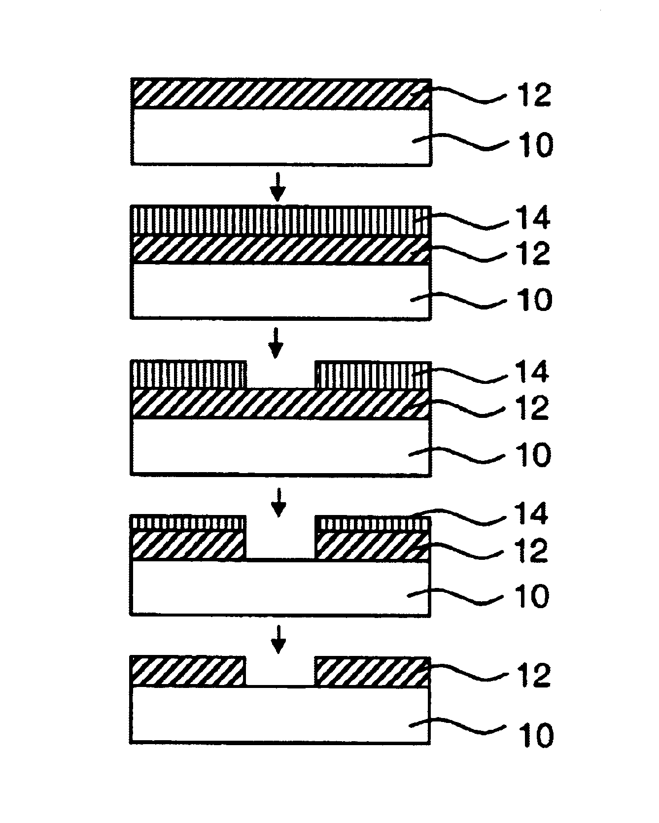
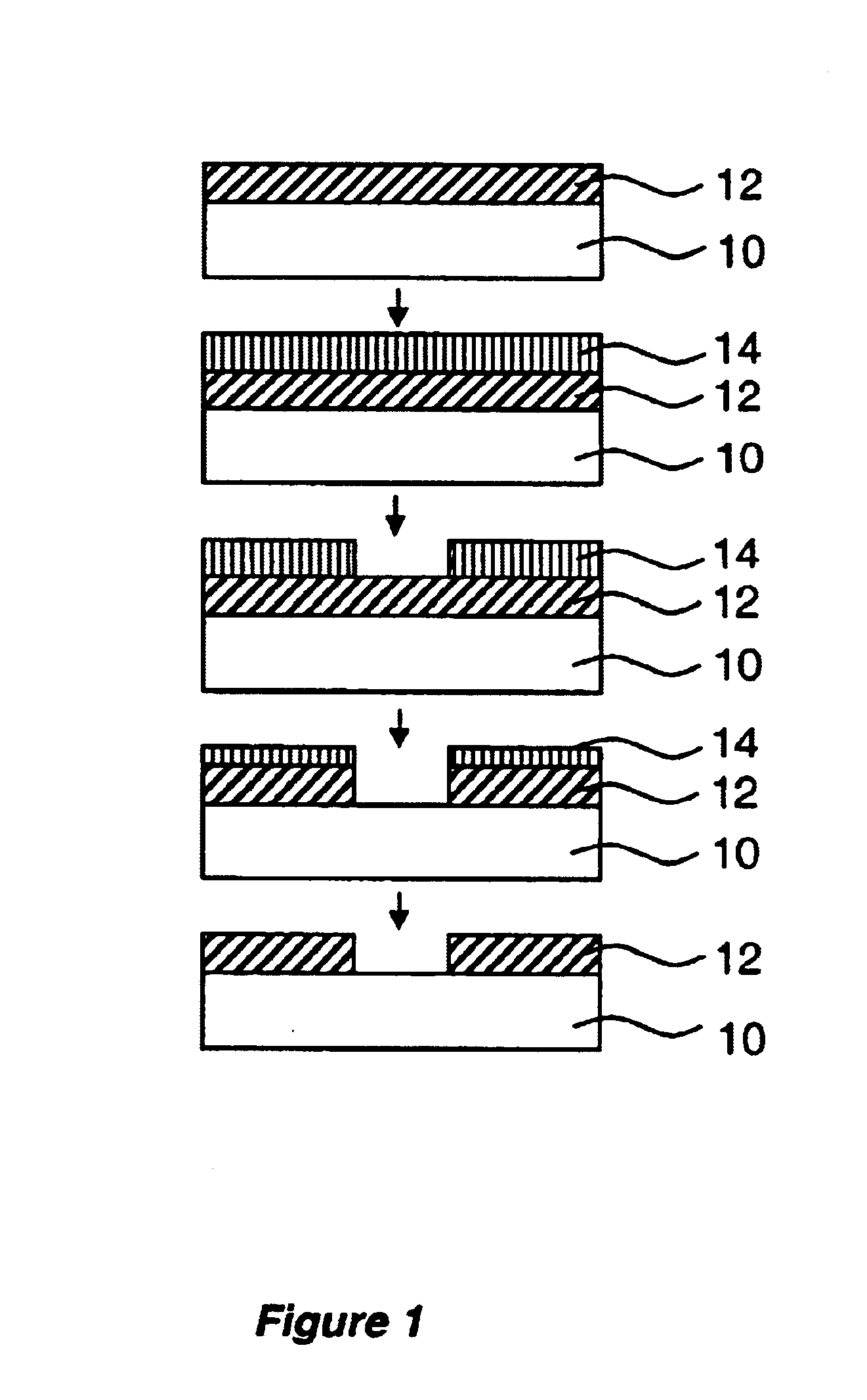
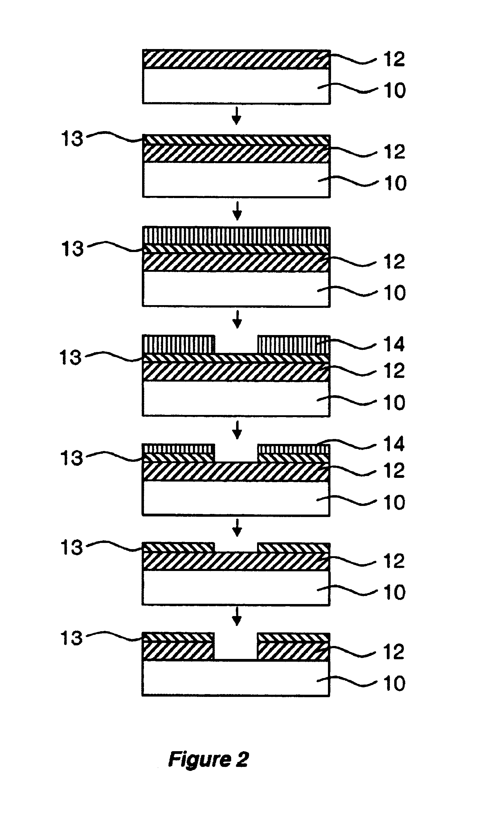
Examples
synthesis examples
MATERIAL SYNTHESIS EXAMPLES
Example 1
[0112]Vinyl 0 mole-%
[0113]Phenyl trichlorosilane (0.6 mol) and methyl trichlorosilane (0.4 mol) are dissolved in dehydrated DCM (800 ml). The solution is added drop wise into a flask containing excess of water (45 mol) while stirring the solution. After addition of the water, the solution stirred for 1 hour at the room temperature. The solution is neutralized by water extraction for 12 times and finally volatile components are evaporated with rotary evaporator. (After evaporation the mixture is stirred at the room temperature under high vacuum until refractive index of the material is in excess of 1). After vacuum treatment dehydrated 300 w-% of mesitylene is added into the material as for process solvent and the material is carefully homogenized. Appropriate initiators are added and dissolved into the mixture. Finally, the material is filtered.
example 2
[0114]Vinyl 5 mole-%
[0115]Vinyl trichlorosilane (0.05 mol), phenyl trichlorosilane (0.57 mol) and methyl trichlorosilane (0.38 mol) are dissolved in dehydrated DCM (800 ml). The solution is added drop-wise into a flask containing excess of water (45 mol) while stirring the solution. After addition of the water, the solution stirred for 1 hour at the room temperature. The solution is neutralized by water extraction for 12 times and finally volatile components are evaporated with rotary evaporator. After vacuum treatment, dehydrated 300 w-% of mesitylene used as process solvent is added into the material and the material is carefully homogenized. Appropriate initiators are added and dissolved into the mixture. Finally the material is filtered.
example 3
[0116]Vinyl 10 mole-%
[0117]Vinyl trichlorosilane (0.10 mol), phenyl trichlorosilane (0.54 mol) and methyl trichlorosilane (0.36 mol) are dissolved in dehydrated DCM. The solution is added drop-wise into a flask containing excess of water (45 mol) while stirring the solution. After addition of the water, the solution stirred for 1 hour at the room temperature. The solution is neutralized by water extraction for 12 times and finally volatile components are evaporated with rotary evaporator. After vacuum treatment dehydrated 300 w-% of mesitylene is added into the material as for process solvent and the material is carefully homogenized. Appropriate initiators are added and dissolved into the mixture. Finally the material is filtered.
PUM
| Property | Measurement | Unit |
|---|---|---|
| thickness | aaaaa | aaaaa |
| dielectric constant | aaaaa | aaaaa |
| dielectric constant | aaaaa | aaaaa |
Abstract
Description
Claims
Application Information