Optical interconnection circuit among wavelength multiplexing chips, electro-optical device, and electronic apparatus

a technology of optical interconnection circuit and wavelength multiplexing chip, which is applied in the direction of waveguides, instruments, semiconductor lasers, etc., can solve the problems of complicated connections between optical parts, such as light emitting elements and light receiving elements, and the signal transmission speed substantially reaches its limit, so as to achieve high speed, low price, and high performance electronic

Inactive Publication Date: 2006-01-03
SEIKO EPSON CORP
View PDF7 Cites 13 Cited by
  • Summary
  • Abstract
  • Description
  • Claims
  • Application Information

AI Technical Summary

Benefits of technology

[0012]According to an aspect of the present invention, it is possible to provide extremely compact wavelength multiplexing transmission devices because it is possible to extremely miniaturize the micro-tile shaped elements (for example, to have areas of several hundred micrometers square or less and thickness of several ten micrometers or less). It is possible to provide easily fabricated wavelength multiplexing transmission devices because it is possible to use the micro-tile shaped element as a data transmission device among integrated circuit chips.
[0044]According to an aspect of the present invention, for example, it is possible to provide compact electronic apparatuses capable of displaying high quality pictures at low prices by applying the optical interconnection circuit among the wavelength multiplexing chips to a display device.

Problems solved by technology

However, in buses to connect the CPUs to peripheral devices, such as memories, signal transmission speed substantially reaches its limit thereby becoming a bottleneck in the processing speed of computers.
However, when optical fiber is used as the optical transmission device, connections between optical parts, such as a light emitting element and a light receiving element, are complicated.
Therefore, it costs too much and takes long to fabricate the optical transmission device.
Also, it is difficult to miniaturize the optical transmission device.
However, input and output structures suitable for the optical waveguide have not yet been found.
Optical transmission devices that are so minute and easily fabricated as to be applied to plane display devices or computers have not yet been realized.

Method used


Image

  • Optical interconnection circuit among wavelength multiplexing chips, electro-optical device, and electronic apparatus
  • Optical interconnection circuit among wavelength multiplexing chips, electro-optical device, and electronic apparatus
  • Optical interconnection circuit among wavelength multiplexing chips, electro-optical device, and electronic apparatus

Examples


first exemplary embodiment

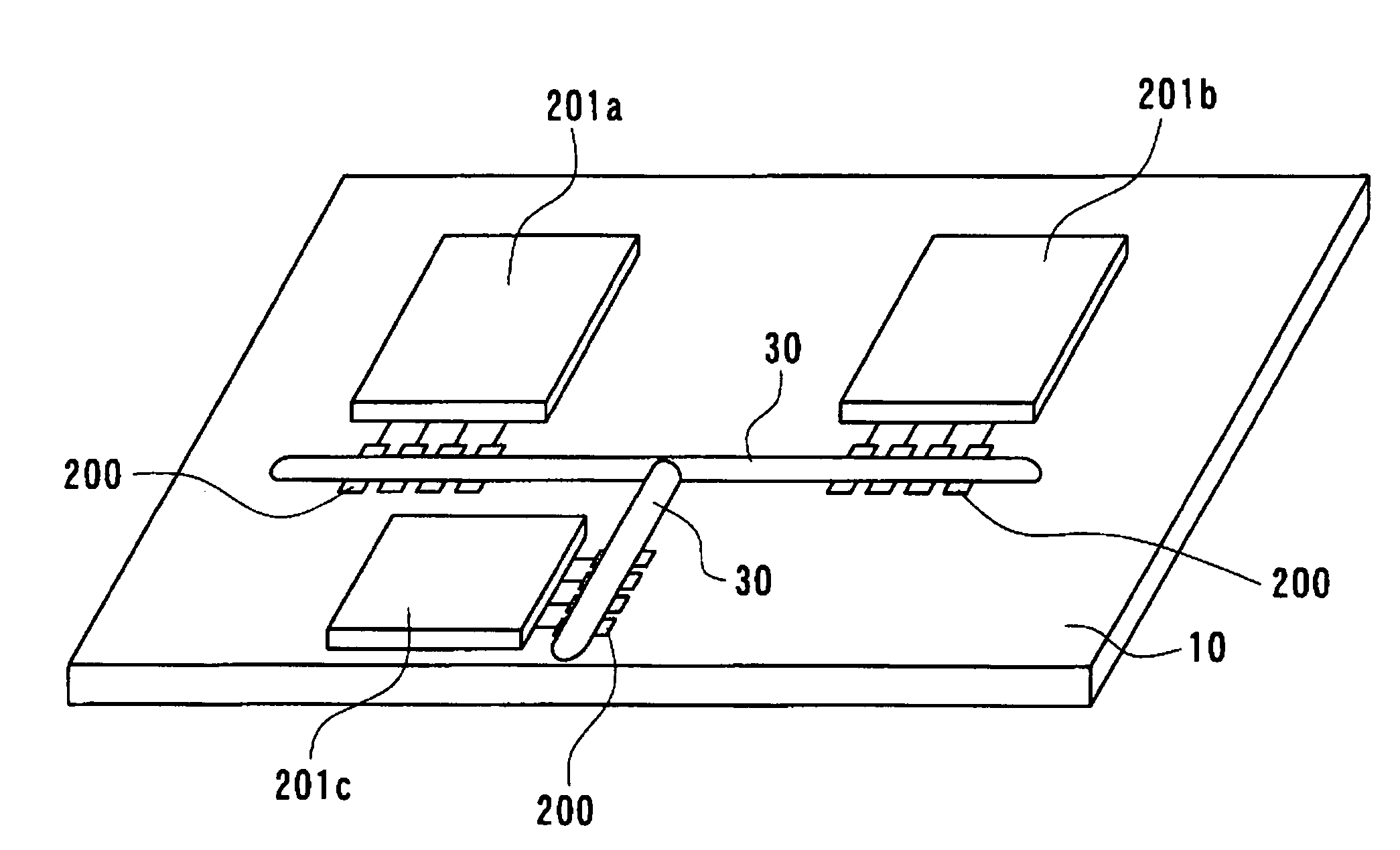
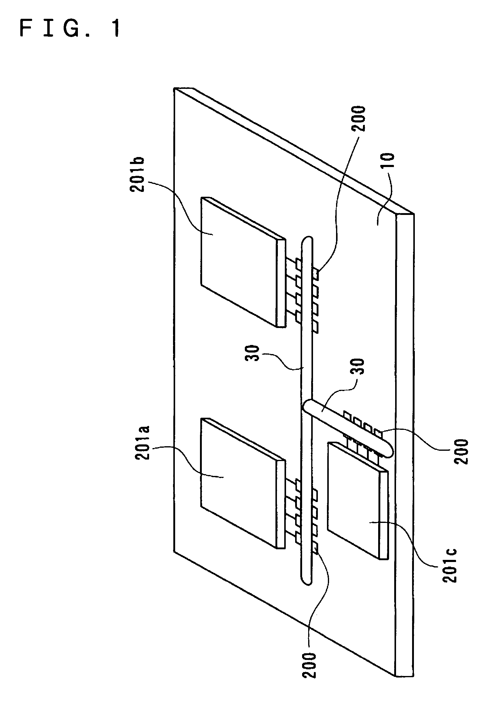
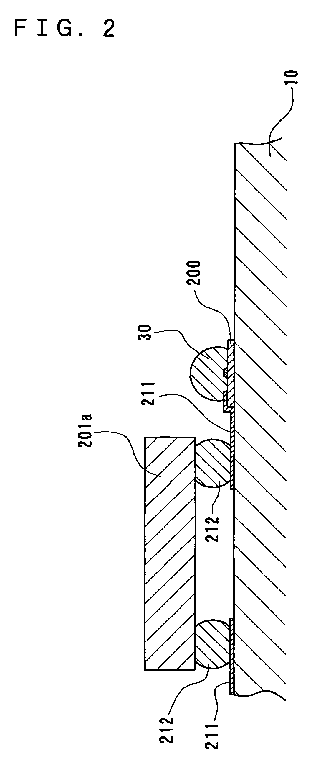
[0076]FIG. 1 is a perspective view illustrating an optical interconnection circuit among wavelength multiplexing chips in accordance with a first exemplary embodiment of the present invention. FIG. 2 is a cross-sectional view of a main portion of the optical interconnection circuit among wavelength multiplexing chips illustrated in FIG. 1.

[0077]A plurality of integrated circuit chips (LSI chips or IC chips) 201a, 201b, and 201c are mounted on the surface of a substrate 10. The integrated circuit chips 201a, 201b, and 201c form a CPU, a memory circuit, an image signal processing circuit, an image signal driving circuit, a communication I / O, various interface circuits, an analog-to-digital (A / D) converter, and a digital-to-analog (D / A) converter. In FIG. 1, three integrated circuit chips 201a, 201b, and 201c are mounted on the substrate 10. However, the present invention is not limited thereto. Glass epoxy, ceramic, glass, plastic, semiconductor, polyimide, and silicon can be used as ...

second exemplary embodiment

[0086]An application example of an optical interconnection circuit among wavelength multiplexing chips according to a second exemplary embodiment of the present invention will now be described with reference to FIGS. 3 to 5. According to the present exemplary embodiment, a timing control circuit and a driver circuit of a flat panel display (FPD) are connected to each other by an optical waveguide 30. FIG. 3 is a circuit schematic of a flat panel display, which illustrates an application example of the optical interconnection circuit among wavelength multiplexing chips according to the second exemplary embodiment of the present invention.

[0087]The substrate 10 is a constituent of the flat panel display. Glass and plastic may be used as the substrate 10. A timing control circuit 222, a plurality of (for example, four) data line driver circuits 223-1, 223-2, 223-3, and 223-4, a plurality of (for example, four) scanning line driver circuits 224-1, 224-2, 224-3, and 224-4, and a pixel ma...

example of application

[0173]Hereinafter, an example of the application of the optical interconnection circuit among wavelength multiplexing chips according to an aspect of the present invention will be described.

[0174]For example, the on-chip optical interconnection circuits of the above-described exemplary embodiments are used as a signal transmission device of an optoelectronics integrated circuit system. A computer is used as the optoelectronics integrated circuit system. Next, integrated circuit chips constituting a CPU are formed on the substrate 10, and integrated circuit chips constituting a storage device are formed on the substrate 10. Although signal processing in the CPU and the storage device is performed using electrical signals, the optical interconnection circuit among wavelength multiplexing chips of the above-described exemplary embodiment is applied to the data transmission between IC chips.

[0175]As a result, in accordance with the present application in simple and easy configuration, i...


PUM

PropertyMeasurementUnit
thicknessaaaaaaaaaa
thicknessaaaaaaaaaa
thicknessaaaaaaaaaa

Abstract

To provide an optical interconnection circuit among wavelength multiplexing chips, capable of increasing signal transmission speed and of being easily made minute thereby being simply and easily fabricated, an electro-optical device, and an electronic apparatus, an optical interconnection circuit among wavelength multiplexing chips, which is disposed on a substrate, includes micro-tile shaped elements having a light emitting function or a light receiving function with wavelength selectivity.

Description

BACKGROUND OF THE INVENTION[0001]1. Field of Invention[0002]The present invention relates to an optical interconnection circuit among wavelength multiplexing chips, an electro-optical device, and an electronic apparatus.[0003]2. Description of Related Art[0004]Electro-luminescence panels (ELPs), plasma display panels (PDPs), and liquid crystal displays (LCDs) are recently used as plane display devices. In such plane display devices, a technology of using light to transmit signals is used in order to address the problem of signal delay caused by an increase in the sizes of the plane display devices and large capacity display.[0005]In computers, operation speed (an operation clock) inside CPUs increases year by year, as the internal structures of integrated circuits become minute. However, in buses to connect the CPUs to peripheral devices, such as memories, signal transmission speed substantially reaches its limit thereby becoming a bottleneck in the processing speed of computers. Wh...

Claims


Application Information

Patent Timeline
Patent Type & Authority Patents(United States)
IPC IPC(8): G02B6/30H04B10/12G02B6/122G02B6/42G02B6/13G02B6/34G02B6/43G02F1/133G02F1/1345G02F1/135G06F3/00H01L21/60H01L31/0232H01L33/30H01L33/48H01L51/50H01S5/022H04B10/00H04B10/275H04B10/278H04B10/524H04B10/572H04B10/80
CPCG02B6/43H01L24/24H01L24/82G02B6/4214G02B6/4246H01L2224/1329H01L2224/16227H01L2224/133H01L2224/131H01L2224/82102H01L2221/68354H01L2221/68368H01L2224/24051H01L2224/24226H01L2224/76155H01L2224/83001H01L2224/83192H01L2224/92244H01L2924/01004H01L2924/01012H01L2924/01013H01L2924/01029H01L2924/0103H01L2924/01046H01L2924/09701H01L2924/10329H01L2924/14H01L2924/30105H01L2924/01005H01L2924/01006H01L2924/01024H01L2924/01033H01L2924/01047H01L2924/014H01L2924/12041Y10S385/901H01L2924/00014H01L2224/16225H01L2924/12042H01L2924/12043H01L2924/00
Inventor KONDO, TAKAYUKI
Owner SEIKO EPSON CORP
Why Eureka
Try Eureka