Semiconductor integrated circuit device

a technology of integrated circuits and semiconductors, applied in semiconductor devices, digital storage, instruments, etc., can solve the problems of difficult to stably set the phase change memory, difficult to reduce the current, and the phase change portion is overheated, so as to prevent re-amorphization, reduce the resistance of the phase change portion, and increase the current amount

Inactive Publication Date: 2006-10-17
RENESAS ELECTRONICS CORP
View PDF12 Cites 80 Cited by
  • Summary
  • Abstract
  • Description
  • Claims
  • Application Information

AI Technical Summary

Benefits of technology

[0013]On the other hand, in a setting operation, as shown in FIG. 5, the gate voltage of the selection transistor QM is set, for example, at one half of VDD and a pulse voltage is applied. Before the setting operation, a phase change portion 2 is in an amorphous phase of high resistance and therefore almost of all of the applied voltage is fed to the phase change portion. Upon occurrence of crystallization, the resistance of the phase change portion becomes lower, so that the amount of current increases. However, since the gate voltage of the selection transistor QM is low, the amount of current flowing through the phase change portion is limited, with the result that the phase change portion is not overheated and thus prevented from re-amorphization. As to the gate voltage applied to the selection transistor QM, it goes without saying that an optimum value is selected in view of the performance of the selection transistor and the composition of the phase change material.
[0015]With a semiconductor integrated circuit device using the technique of the present invention, it is possible to implement a highly reliable a non-volatile semiconductor memory. If this device is mounted on one and same substrate together with a semiconductor logic unit, it is possible to provide a highly reliable high function-incorporated microcomputer. The device in question can also be provided as a single chip.

Problems solved by technology

Typical of the non-volatile memory is FLASH memory, which, however, is used as a programmable ROM because the speed thereof is essentially low.
However, if a constant voltage source is used, as shown in FIG. 3, the phase change portion crystallizes into a state of low resistance and a large current flows in accordance with the Ohm's law, so that the phase change portion is overheated.
As a result, the temperature of the phase change portion exceeds its melting point and thereafter the phase change portion is quenched, whereby there again arises the possibility of amorphization.
Thus, with the constant voltage source, it has so far been difficult to set the phase change memory stably.

Method used


Image

  • Semiconductor integrated circuit device
  • Semiconductor integrated circuit device
  • Semiconductor integrated circuit device

Examples


first embodiment

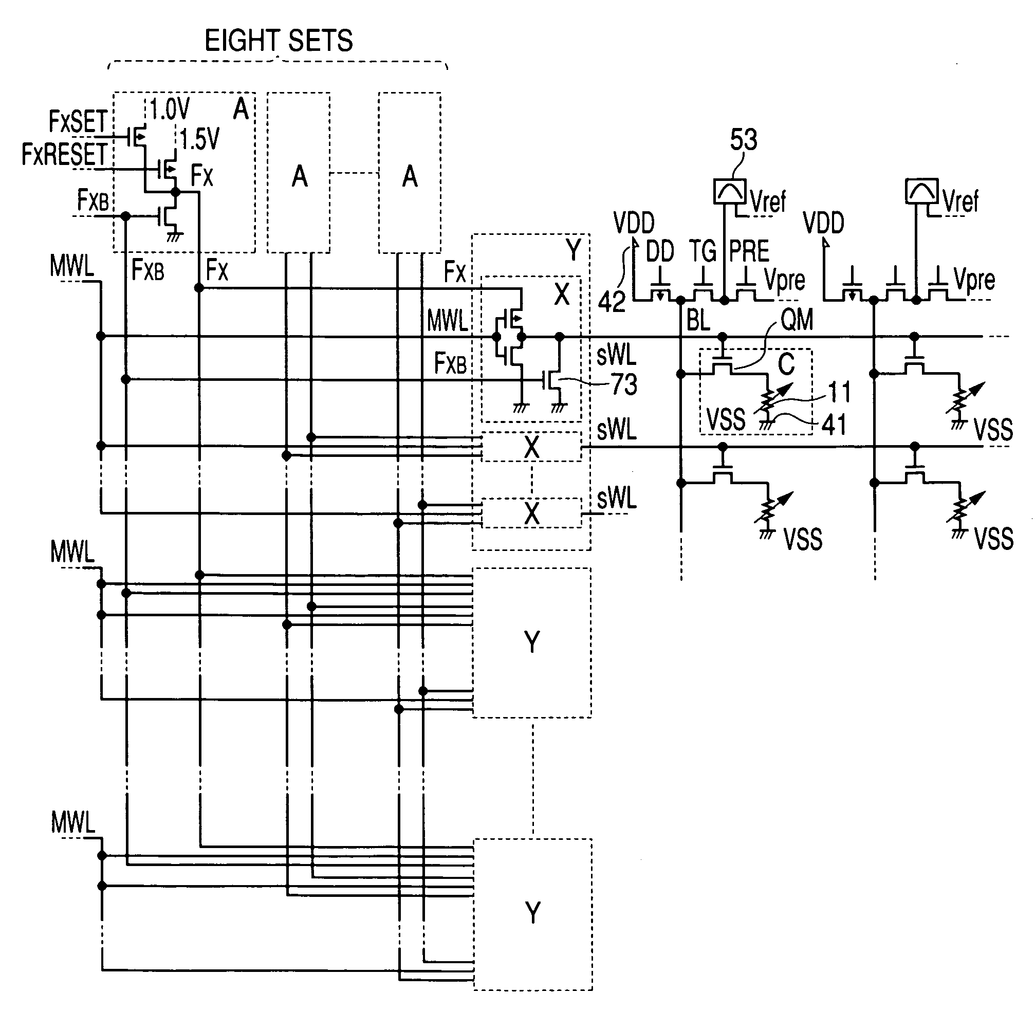
[0028]In this embodiment, how the memory array shown in FIG. 1 operates will be described in detail. A memory cell C is composed of one information storage portion and one selection transistor. The selection transistor is an MIS type transistor. Although only four memory cells are described in FIG. 1, this is because of simplification for showing the problem and the principle of the present invention. Circuit elements which constitute blocks in this embodiment, though not specially limited, are typically formed on such a single semiconductor substrate as a single crystal silicon by a semiconductor integrated circuit technology such as a known CMOS (a complementary MOS transistor). As the material of the information storage portion, there is used a phase change material, especially chalcogenide. A sub-word line driver Y drives eight sub-word lines sWL per piece. Thirty-two sub-word line drivers Y are arranged, while a total of 256 sub-word lines sWL are laid.

[0029]Prior to write, FXB...

second embodiment

[0046]In this embodiment there is proposed a method using a circuit shown in FIG. 8 as a circuit which prevents re-amorphization and is thereby effective in stabilizing the setting operation. This circuit is characterized by comprising current mirror circuits 281 and 282. The current mirror circuit 281 can supply 10 μA current, while the current mirror circuit 282 can supply 100 μA current.

[0047]Before rewrite, FXB, TG, and PRE, are at an increased potential, while FX1, sWL, MWL, and DD, are at the ground potential VSS. The transistors 283 and 284 are OFF. BL is held at the precharge potential Vpre.

[0048]To reset the memory cell C, FXB, PRE, and TG, are deactivated, while FXl and DD are activated. Next, the transistor 284 is turned ON. Then, MWL is activated to set the gate voltage of the selection transistor QM at VDD. With this operation, 100 μA current for heating the phase change portion 211 to above its melting point flows through the phase change portion.

[0049]Of course, a lar...

third embodiment

[0052]In the first embodiment the phase change portion is disposed between the selection transistor and the ground potential, but in this third embodiment a selection transistor is disposed between a phase change portion and the ground potential.

[0053]A cell array of this embodiment is shown in FIG. 9. A peripheral circuit portion is the same as in the first embodiment. A memory cell D comprises a phase change portion PC and a selection transistor QM. In this embodiment, the bias potential of the selection transistor QM can be held at the common line potential VSS, so that a back bias is not imposed on the selection transistor QM and hence the selection transistor can be driven at a low voltage. Besides, since the common line can be laid without using a diffusion layer, the memory cell area can be diminished.

[0054]However, due to the wiring capacity, when the bit line potential varies, a slight amount of current flows also through the phase change portion of the memory cell with the...


PUM


Abstract

In a non-volatile phase change memory, information is recorded by utilizing a change in resistance of a phase change portion. When the phase change portion is allowed to generate Joule's heat and is held at a specific temperature, it goes into a state of a low resistance. When the gate voltage of a memory cell selection transistor QM is controlled to afford a low resistance state, the maximum amount of current applied to the phase change portion is limited by the application of a medium-state voltage to the control gate, thereby avoiding overheating of the phase change portion.

Description

CLAIM OF PRIORITY[0001]The present invention claims priority from Japanese application JP2003-406802, filed on Dec. 5, 2003, the content of which is hereby incorporated by reference into this application.BACKGROUND OF THE INVENTION[0002]1. Field of the Invention[0003]The present invention relates to a semiconductor integrated circuit device and more particularly to a technique applicable effectively to a high-density integrated memory circuit formed by using a phase change material, a logic mixed memory having a memory circuit and a logic circuit on one and same semiconductor substrate, or a semiconductor integrated circuit device having an analog circuit. Particularly, the present invention is concerned with a non-volatile high-speed random access memory.[0004]2. Description of Related Art[0005]The growth of the non-volatile memory market under the demand for mobile devices typified by portable telephones is remarkable. Typical of the non-volatile memory is FLASH memory, which, how...

Claims


Application Information

Patent Timeline
Patent Type & Authority Patents(United States)
IPC IPC(8): G11C17/18G11C13/00G11C11/00G11C13/02G11C16/02G11C17/00H01L27/10
CPCG11C11/56G11C11/5678G11C13/0004G11C13/003G11C13/004G11C13/0069G11C2213/79G11C2013/0054G11C2013/0071G11C2013/0078G11C2013/009G11C2213/76G11C13/00G11C13/02
Inventor KUROTSUCHI, KENZOTAKAURA, NORIKATSUTONOMURA, OSAMUTERAO, MOTOYASUMATSUOKA, HIDEYUKITAKEMURA, RIICHIRO
Owner RENESAS ELECTRONICS CORP
Why Eureka
Try Eureka