Polymeric microfabricated fluidic device suitable for ultraviolet detection

a microfluidic device and polymer technology, applied in the field of polymer-based microfluidic devices, can solve the problems of inability to disclose the dimensions of injection molding at less than 100 m, the limitations of silicon for this application, and the disadvantages of each of these polymers, so as to increase the cross sectional dimension and increase the optical path length

Inactive Publication Date: 2006-12-19
EI DU PONT DE NEMOURS & CO
View PDF20 Cites 41 Cited by
  • Summary
  • Abstract
  • Description
  • Claims
  • Application Information

AI Technical Summary

Benefits of technology

[0017]The improvement also comprises a means of rendering the Teflon AF® surface hydrophilic and a means for bonding the two said planar substrates for fluidic transport. The improvement also enables the microfluidic devices to be used when ultraviolet spectrophotometry is used for detecting analytes moving through the channels.
[0019]Further disclosed is a substantially polymeric microfluidic device comprising a body having a reagent-bearing channel, at least one section of which has an increased cross-section dimension with respect to other sections of said reagent-bearing channel. This increased dimension provides an increased optical path length through the reagent for the purpose of increasing the sensitivity of any optical based analysis conducted on the reagent in the channel.
[0021]In one embodiment of the microfluidic device, at least one section of one of the at least first and second intersecting channels has an increased cross sectional dimension with respect to other sections of said channel, to provide an increased optical path length when used in an ultraviolet detection arrangement.

Problems solved by technology

It is known that silicon has limitations for this application because the electric field needed to drive the fluid in a capillary electrophoretic separation device often exceeds the dielectric breakdown field of silicon.
However, injection molding at dimensions smaller than 100 μm has not been disclosed.
Each of these polymers suffers disadvantages.
PDMS and polyurethane are not injection moldable, PVC is typically chemically impure, PMMA and polycarbonate are not UV-transparent and PTFE is typically not optically clear.
Electroconductivity detection is susceptible to contamination problems on the electrode and is difficult to operate in capillary electrophoresis because of the presence of the high electrophoretic voltage in the background.
The use of Pyrex® in microfluidic devices has hindered the application of these devices to UV spectroscopy.
Likewise, the most popular polymer resins, such as PMMA, used in visible wavelength optical applications are not particularly transparent below three hundred nanometers (300 nm).
The other hindrance for incorporating UV spectrophotometry as the detection technique is that UV sensitivity is several orders of magnitude lower than that of light fluorescence spectroscopy.
Artificial diamond, however, is made by an expensive process.
The tape is not an optimal solution for sealing devices because it has limited mechanical strength, and is generally not UV-transparent.
Prior art polymeric materials are not sufficiently transparent in the ultraviolet.
Polymeric materials suffer from the deficiency of lower thermal conductivity than silicon and glass, the original materials of construction for microfluidic devices.

Method used


Image

  • Polymeric microfabricated fluidic device suitable for ultraviolet detection
  • Polymeric microfabricated fluidic device suitable for ultraviolet detection
  • Polymeric microfabricated fluidic device suitable for ultraviolet detection

Examples


example 1

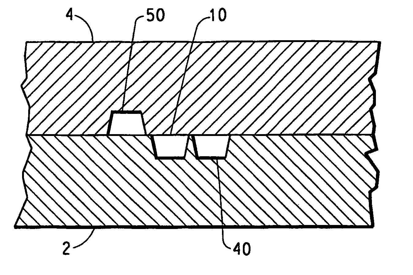
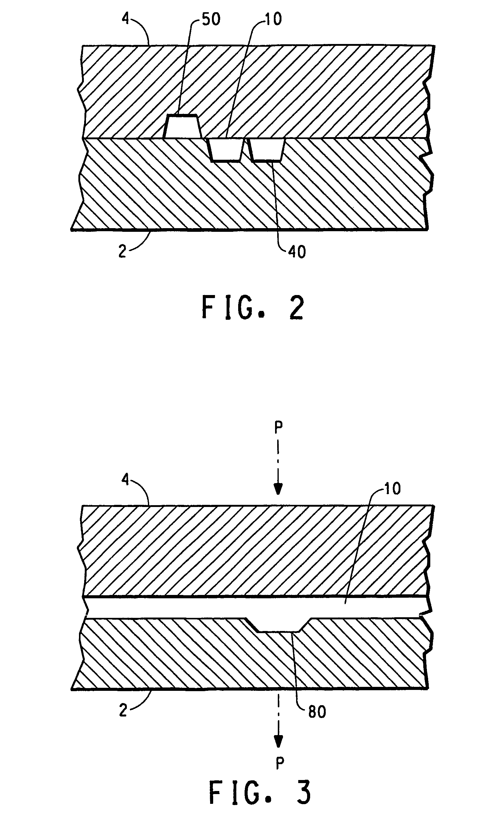
[0042]A three-inch diameter silicon negative master mold insert was fabricated using well-known procedures in the art. This silicon master had 3 separate microfluidic devices on the wafer. Each microfluidic device consisted of a 100-μm wide separation channel and two T-injection junctions. The injection channel was 50 μm wide at the end joining the injection well, and it narrowed down to 20 μm at the junction with the separation channel. This mold insert was attached onto the mold in the injection mold cavity with a double-sided adhesive tape. The injection molder was the horizontal type where the mold is positioned vertically with respect to the motion of the chuck holding the nozzle of the injection molder. In a vertical injection molder, the double-sided tape would not be needed.

[0043]The surface of the mold cavity was heated to about 60° C. Topas® 8007 pellets were outgassed overnight in a vacuum oven at a temperature no greater than 50° C. The resin temperature and nozzle tempe...

example 2

[0049]A nickel mold was fabricated by electroplating a silicon positive having the microfabricated features with nickel. The resulted nickel mold was placed on the lower plate of a press. A ˜2.5″ diameter circular hole was cut out from a 0.004″ thick Kapton® polyimide film. The resulted circular space was placed on the nickel mold so that the microfabricated features on the nickel mold were contained inside the circular space. The temperature of the press was maintained at about 230° C. Teflon AF® granules were placed inside the circular space to slightly over-fill the circular space. Another sheet of Kapton® was placed onto the surface of the Teflon AF® granules. A copper disk slightly larger than the circle was placed on the Kapton® sheet. The press was closed and the pressure was was applied gradually over a few minutes and the pressure was maintained at 1500 psi for 5–6 minutes. The resulting film of Teflon AF® was optically very clear and the microfabricated features were trans...

example 3

[0051]A device made of polydimethylsiloxane (PDMS) was cast containing a 100 micrometer wide separation channel with a section of the channel, called a “bubble”, having a vertical dimension of 200 microns. The PDMS device was bonded to a quartz plate with built-in platinum electrodes for use as an electrophoresis device. A supply reservoir was connected to one end and a waste reservoir was connected to the other end of the separation channel. The bubble was aligned with a 200 micron long by 100 micron wide optical detection slit. A standard solution of 400 micromolar para-hydroxycinnamic acid in methanol was injected into the 100 micron-width separation channel filled with a pH 9.3 aqueous borate buffer through a 50 micron-wide cross channel in the T-injection junction, similar to FIG. 1. A potential difference of 3.5 kV was applied between the electrodes in contact with the supply reservoir filled with a pH 9.3 aqueous borate buffer, and in contact with the waste reservoir. Ultravi...


PUM

PropertyMeasurementUnit
wavelengthsaaaaaaaaaa

Abstract

A polymer-based microfluidic device and its manufacturing methods. This microfluidic device is suitable for chromatographic and electrophoretic separations in which the detection of the components in the fluid is by means of ultraviolet (UV) spectroscopy. The device further comprises at least one cooling channel adjacent the separation channel, said cooling channel conducting a cooling fluid through the device for removing heat from the the separation channel. At least one section of the separation channel has an increased cross-sectional dimension with respect to other sections of said channel to provide an increased optical path length when the device is used in an ultraviolet detection arrangement.

Description

[0001]This application claims the benefit of priority of International Application No. PCT / US01 / 30974, filed Oct. 3, 2001, which in turn claims benefit of priority of U.S. Provisional Application 60 / 238,066, filed Oct. 5, 2000 and U.S. Provisional Application 60 / 238,067, filed Oct. 5, 2000.FIELD OF THE INVENTION[0002]This invention relates to a polymer-based microfluidic device and its manufacturing methods. This microfluidic device is suitable for chromatographic and electrophoretic separations in which the detection of the components in the fluid is by means of ultraviolet (UV) spectroscopy and for chromatographic and electrophoretic separations in which the detection of the components in the fluid is by means of visible light, fluorescence, chemiluminescence or scattering or by means of electrochemical and electroconductivity detection.TECHNICAL BACKGROUND OF THE INVENTION[0003]There is a large volume of literature on the manufacturing of planar microfabricated devices primarily ...

Claims


Application Information

Patent Timeline
Patent Type & Authority Patents(United States)
IPC IPC(8): G01N27/453G01N31/20B01D57/02B01J19/08B01L3/00B01L7/00B03C5/00B81B1/00G01N21/05G01N21/33G01N21/64G01N27/447G01N30/60G01N37/00
CPCB01L3/502707B01L3/50273B01L7/00G01N21/05G01N21/33G01N27/44708G01N27/44721G01N27/44791G01N30/6095B01L3/5027B01L2200/0689B01L2200/12B01L2300/0816B01L2300/0887B01L2300/185B01L2300/1894B01L2400/0418G01N2030/3007G01N30/74G01N2021/0346
Inventor ASHMEAD, JAMES WILLIAMTANG, SAU LAN
Owner EI DU PONT DE NEMOURS & CO
Why Eureka
Try Eureka