Fabrication method for electronic system modules

a technology of electronic system modules and fabrication methods, which is applied in the direction of connection contact member materials, sustainable manufacturing/processing, and final product manufacturing, etc., can solve the problems of not being able to support not being able to meet the requirements of direct bonding of ic chips, and not being able to meet the requirements of direct mounting of bumped devices

Inactive Publication Date: 2007-11-20
SK HYNIX INC
View PDF29 Cites 26 Cited by
  • Summary
  • Abstract
  • Description
  • Claims
  • Application Information

AI Technical Summary

Benefits of technology

[0019]A glass substrate for 5th generation fabrication of LCD circuits is typically 1100 by 1250 mm in area, and 0.7 mm or 1.1 mm thick, which can be used in carrying out the present invention. However, the glass carrier of the current invention can be of any size. The unit manufacturing costs of interconnection circuits and related circuit structures of the current invention are lower if larger glass panels are used. The glass or other rigid carrier provides mechanical support for all of the fabrication, component assembly, cable assembly, test, and rework process steps, and also has excellent dimensional stability. This dimensional stability transfers to the multi-layer interconnection circuits that are built up as a series of films on top of the glass. This transferred dimensional stability is a primary reason that fine line features such as trace width and space of 5 microns are possible with the current invention. It is also important however, that the final version of the interconnection circuit be flexible, because this flexibility allows the use of an epoxy under layer to be avoided, leading to more robust rework processes for removing and replacing defective chips. The flexibility also allows system boards to be folded in compact devices such as cellular phones. Folding requires that the chips be arranged in rows, and the clear area between rows becomes a potential folding line.
[0020]A release agent is applied to a glass panel substrate, except for a clear region near the edges. The clear region is characterized by high adhesion between the glass and the polymer base layer to be subsequently formed on the glass. The high adhesion region provides an anchor that firmly attaches the polymer to the glass around the perimeter of the panel. The release layer creates low adhesion between glass and polymer, so that after a circuit assembly has been built on top, it can be readily peeled off.
[0021]Alternate layers of metal interconnect and dielectric such as a photo-definable polymer are built up on the base layer. Two-level contacts are formed between adjacent metal layers, and stacked contacts are provided between groups of adjacent layers. Preferably each input / output (I / O) pad of an assembled IC chip is a tested node of the multi-layer interconnection circuit. At the center of each I / O pad a stacked contact is preferably created, with stubs at every metal layer, for convenient routing of traces. The base polymer layer, the dielectric layers and the metal layers are flexible, and when the multi-layer interconnection circuit is subsequently removed from the glass panel, it too is flexible. Attached IC chips are usually not flexible (unless thinned down by lapping), but if a folding line on the interconnection circuit is kept clear of IC chips, then the circuit assembly can be folded at the folding line.
[0024]A module cable with high-density interconnections is preferably attached to each circuit assembly while the attached carrier provides dimensional stability. Each circuit assembly is then separated from its glass carrier by peeling the base substrate away from the carrier. A low adhesion force is provided in these regions so that separation can be accomplished without damaging the interconnection circuits or the attached components.

Problems solved by technology

This is not sufficient for direct bonding of IC chips; in fact none of the available printed circuit board technologies can support direct mounting of bumped devices at a pitch of 100 microns or less.
However, the application of IC chip manufacturing facilities to this problem is more than what is required.
The process of cleaning off the epoxy and the residue has often resulted in damage to the fine pitch bonding leads, to the point where they cannot be reliably re-bonded.
However, using the proposed flip chip assembly method, it may be necessary to limit the maximum size of IC chips assembled, to limit the maximum strain induced by thermal mismatch during assembly.

Method used


Image

  • Fabrication method for electronic system modules
  • Fabrication method for electronic system modules
  • Fabrication method for electronic system modules

Examples


second embodiment

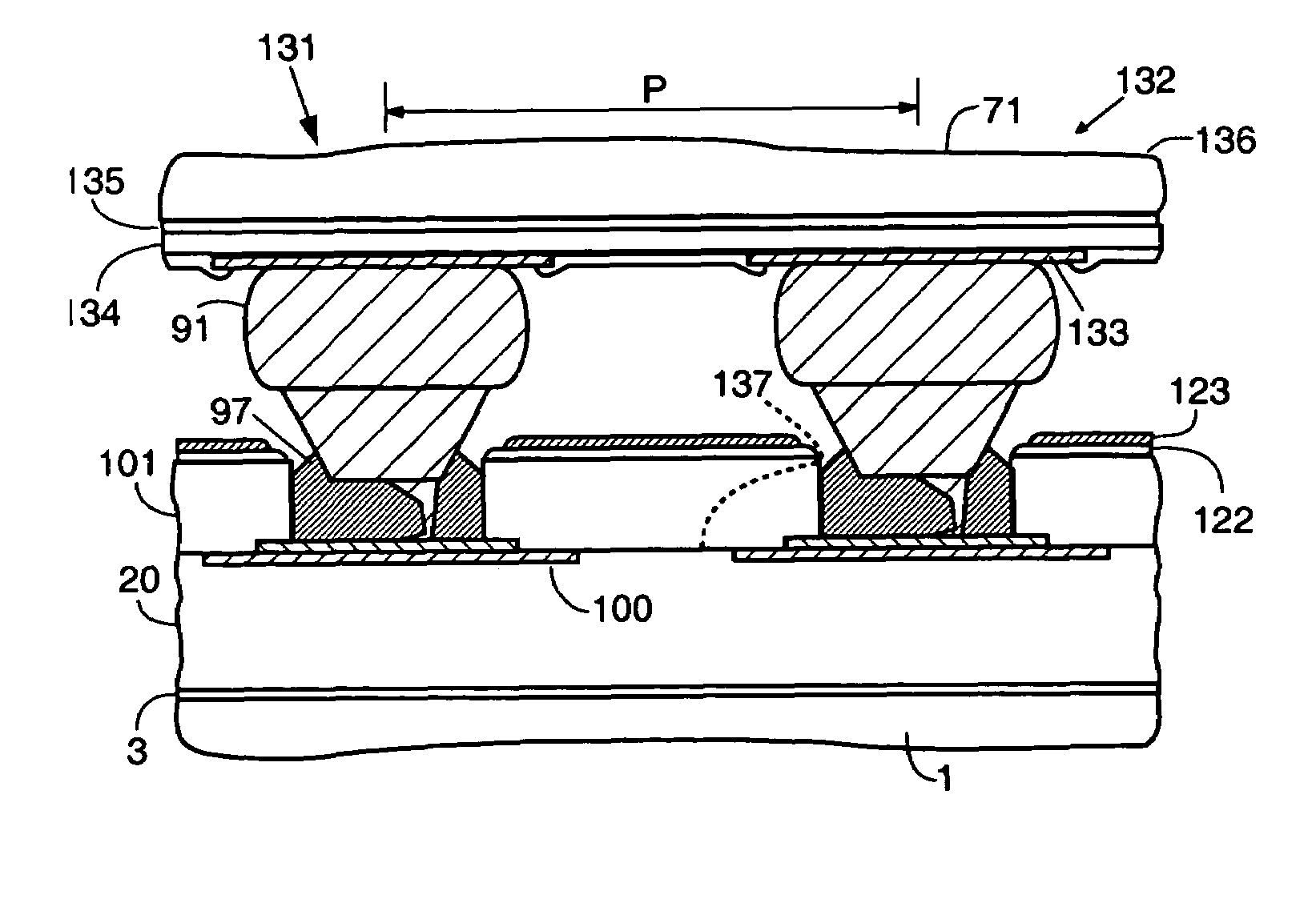
[0071]In FIG. 10A interconnection circuit 20 is shown, including flat I / O pads 100, coated with metallization 95 as previously described. Again, glass carrier 1 is present for dimensional stability. In FIG. 10B a planarizing layer 101 of non-photo-definable polymer such as BCB is formed on top of interconnection circuit 20, at a thickness of approximately 15 microns when cured. Polymer layer 101 is masked and etched using known dry etching techniques to create openings (wells) 102 above the pads. The diameter of the wells is approximately 34 microns in the preferred embodiment. The openings preferably have vertical walls as shown, providing maximum resistance to shear forces in the final assembly (with chips attached). Vertical walls are not generally producible using photo-defined polymers such as photo BCB, and this is why dry etching is used, preferably with an anisotropic etching characteristic as is known in the art. Polymer layer 101 forms the solder paste mask and is typicall...

first embodiment

[0072]It is a primary goal of the current invention to provide flip chip assemblies that can be reworked when a defective chip needs replacement. The process should be simple and effective, and robust enough to perform as many times as may be necessary. Consequently, it is important to choose a solder composition that does not significantly dissolve the stud bump material, does not form brittle intermetallic compounds, and for which the melting point is not significantly increased during assembly or rework cycles. Gold is the preferred material for the stud bumps. As previously described, an example of a solder material that is compatible with gold stud bumps and the flip chip bonding methods proposed herein is indium-based solder Indalloy #290, obtainable from Indium Corporation of America, Utica, N.Y. The amount of paste in a well is approximately 1.5×10⁻⁸ gm in the second preferred embodiment, at a material cost of approximately US$3.48 per gram. For either method of fabricating ...


PUM

PropertyMeasurementUnit
trace widthaaaaaaaaaa
widthaaaaaaaaaa
widthaaaaaaaaaa

Abstract

This specification describes techniques for manufacturing an electronic system module. The module includes flexible multi-layer interconnection circuits with trace widths as narrow as 5 microns or less. A glass panel manufacturing facility, similar to those employed for making liquid crystal display, LCD, panels is preferably used to fabricate the interconnection circuits. A multi-layer interconnection circuit is fabricated on the glass panel using a release layer. A special assembly layer is formed over the interconnection circuit comprising a thick dielectric layer with openings formed at input / output (I / O) pad locations. Solder paste is deposited in the openings using a squeegee to form wells filled with solder. IC chips are provided with gold stud bumps at I / O pad locations, and these bumps are inserted in the wells to form flip chip connections. The IC chips are tested and reworked. The same bump / well connections can be used to attach fine-pitch cables. Module packaging layers are provided for hermetic sealing and for electromagnetic shielding. A blade server or supercomputer embodiment is also described.

Description

RELATED APPLICATIONS[0001]This application is a continuation-in-part of U.S. patent application Ser. No. 10 / 237,640 filed Sep. 6, 2002 which claims priority to U.S. Provisional Application Ser. No. 60 / 318,271 filed Sep. 7, 2001.BACKGROUND OF THE INVENTION[0002]1. Field of the Invention[0003]This invention relates generally to connections between components, and more particularly to connection arrays where each connection in the array includes a bump inserted into a well containing bonding material.[0004]2. Description of the Related Art[0005]The number of input / output (I / O) connections required by integrated circuit (IC) chips is increasing, to several hundred for recent microprocessor chips. As verification of complex designs becomes an increasing portion of the total design activity, it is desirable to increase the I / O count further, to provide access to more internal nodes for testing. Flip chip assembly methods have helped to provide more I / O connections because they provide an ...

Claims


Application Information

Patent Timeline
Patent Type & Authority Patents(United States)
IPC IPC(8): H01L21/00H01L23/498H01L23/538H05K1/00H05K1/11H05K3/00H05K3/34H05K3/46
CPCH01L21/6835H01L23/5386H01L23/5387H01L24/16H01L24/81H05K1/0289H05K1/115H05K3/3436H05K3/363H05K3/4682H01L23/49811H01L2924/3651H01L2221/68345H01L2224/1134H01L2224/13099H01L2224/13144H01L2224/81052H01L2224/81191H01L2224/8121H01L2224/81815H01L2924/01013H01L2924/01015H01L2924/01018H01L2924/01027H01L2924/01029H01L2924/01039H01L2924/01049H01L2924/01051H01L2924/01074H01L2924/01075H01L2924/01078H01L2924/01079H01L2924/01082H01L2924/01327H01L2924/14H01L2924/3011H01L2924/3025H05K3/007H05K3/3484H05K3/4015H05K2201/0367H05K2201/0379H05K2201/09472H05K2201/09509H05K2201/10674H05K2203/016H05K2203/0568H01L2224/13109H01L2924/01005H01L2924/01006H01L2924/01019H01L2924/01033H01L2924/01047H01L2924/0105H01L2924/014H01L2224/16237H01L2224/11332Y10T29/49155H01L2224/05573H01L2224/45144H01L2924/00014H01L2924/15788H01L2924/351H05K3/3485Y02P70/50H01L2924/00H01L2224/05599
Inventor SALMON, PETER C.
Owner SK HYNIX INC
Why Eureka
Try Eureka