
Fabrication system, light-emitting device and fabricating method of organic compound-containing layer

a technology of organic compound and light-emitting device, which is applied in the direction of vacuum evaporation coating, electroluminescent light sources, coatings, etc., can solve the problems of uneven film thickness between a center portion and a marginal portion of a substrate, the efficiency of utilizing expensive el materials is extremely low, and the cost of fabricating a light-emitting device becomes very high, so as to achieve the reduction of the thermal coefficient, the effect of reducing th

Inactive Publication Date: 2008-05-27
SEMICON ENERGY LAB CO LTD
View PDF57 Cites 18 Cited by
  • Summary
  • Abstract
  • Description
  • Claims
  • Application Information

AI Technical Summary

Benefits of technology

[0017]Low deposition rate materials can be deposited in short time with high throughput by means of filling same materials in plural crucibles and depositing them simultaneously. In case of a material that is changed in a film quality depending on the deposition rate is deposited, uniform film quality and thickness can be obtained by filling same materials in plural crucibles and depositing them simultaneously. Further, a region where evaporation materials are mixed (mixed region) on an interface between each film of an EL layer having laminated structure can be formed by filling same materials in plural crucibles and depositing them simultaneously.
[0069]In each above described structure, a thin film containing above described carbon as its main component is a diamond like carbon film (also referred to as DLC film), a CN film, or an amorphous carbon film with 3-10 nm thickness. The DLC film has a SP3 bond as a carbon-carbon bond in a short range order, however, an amorphous structure at the macro level. A constitution of the DLC film is carbon of 70 to 95 atomic % and hydrogen of 5 to 30 atomic %. The DLC film is extremely solid and has high insulation performance. In addition, the DLC film is chemically stable and hard to change. The DLC film has a thermal conductivity of 200 to 600 W / mk enabling dissipating exothermic heat during driving. Such DLC film has a characteristic of having low gas permeability such as moisture or oxygen. In addition, it is known that the DLC film has a degree of hardness of 15 to 25 Gpa by a microhardness tester.

Problems solved by technology

Therefore, in forming the EL layer, an efficiency of utilizing the expensive EL material is extremely low i.e. about 1% or less and fabricating cost of a light-emitting device becomes very high.
Also, in using a large area substrate, it may be a problem that the film thickness between a center portion and a marginal portion of a substrate is uneven.
Further, the vapor deposition system has a structure for a rotation of a substrate and therefore, there is a limit in the vapor deposition system aiming at a large area substrate.
Further, there is a problem that the EL material is easily oxidized and deteriorated due to a presence of oxygen or water.
However, in forming a film by a vapor deposition method, a predetermined amount of a evaporation material put into a vessel (glass bottle) is taken out and transferred to a vessel (representatively, crucible, or vapor deposition boat) installed at a position opposite to an object to be deposited at inside of a vapor deposition system and there is a concern that the evaporation material is mixed with oxygen or water or an impurity in the transferring operation.
However, when the glove is provided at the pretreatment chamber, the chamber cannot be subjected to vacuum, the operation is carried out under atmospheric pressure and there is a high possibility of mixing an impurity.
Even when the transferring operation is carried out at inside of the pretreatment chamber subjected to a nitrogen atmosphere, it is difficult to reduce moisture or oxygen as little as possible.
Further, although it is conceivable to use a robot, since the evaporation material has a powder-like shape and therefore, it is very difficult to fabricate the robot for carrying out the transferring operation.
Therefore, it is difficult to perform steps of forming an EL device, in other words, from a step of forming an EL layer above a lower electrode to a step of forming an upper electrode, by an integrated closed system preventing an impurity from being mixed.

Method used


Image

  • Fabrication system, light-emitting device and fabricating method of organic compound-containing layer
  • Fabrication system, light-emitting device and fabricating method of organic compound-containing layer
  • Fabrication system, light-emitting device and fabricating method of organic compound-containing layer

Examples


embodiment mode 1

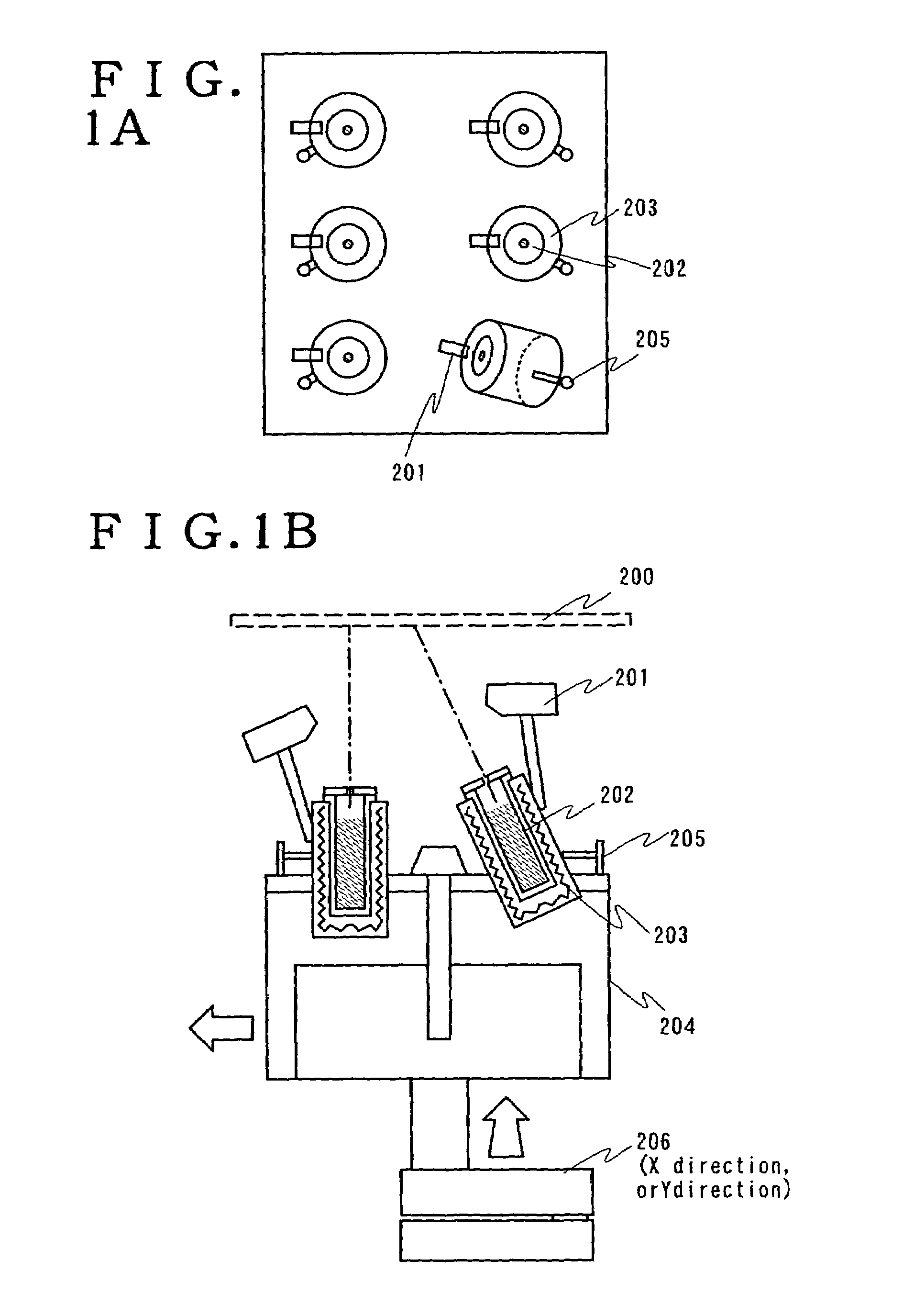
[0103]An evaporation source holder that is moved in X-direction or Y-direction in a deposition chamber will be described with reference to FIG. 1A and FIG. 1B.

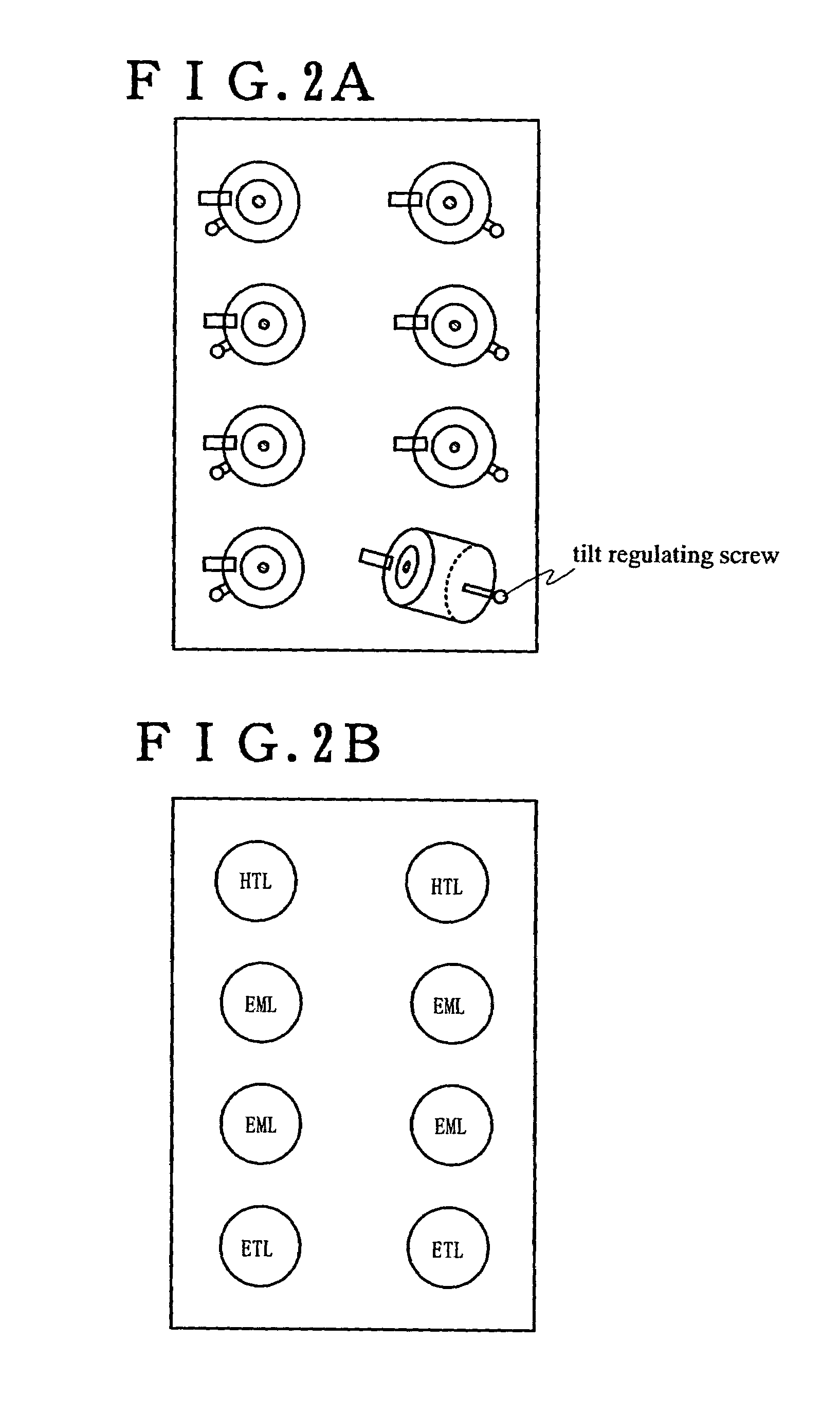
[0104]FIG. 1A is a top surface view showing an evaporation source holder 204 having six containers (crucibles) 202. FIG. 1B is a cross-sectional view showing the evaporation source holder 204. Each six crucible has a film-thickness monitor 201. Viewed from the cross-section of the evaporation source holder, one of a container is tilted using a tilt regulating screw 205 against the surface of a substrate 200. Both a tilt regulating screw 205 and a film thickness monitor 201 are located at the side of the container body. The container can be tilted with a heater 203. The heater 203 is used here to carry out vapor deposition by resistance heating.

[0105]The vapor deposition can be controlled by using a sliding type shutter (not shown). For example, when an evaporation holder is not beneath the substrate 200, the vapor deposition c...

embodiment mode 2

[0111]FIG. 3A and FIG. 3B are a views showing an evaporation holder that has no shutter.

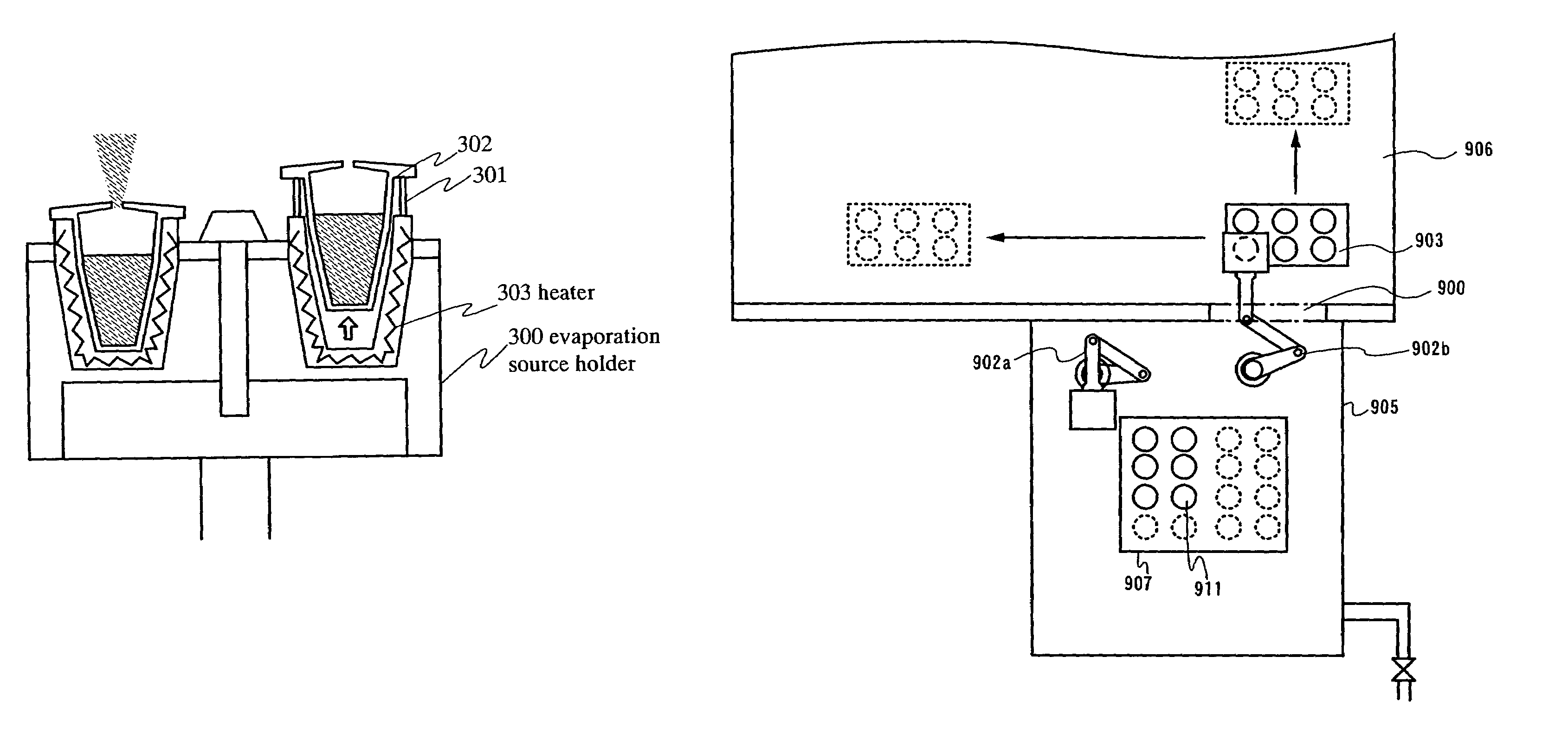
[0112]FIG. 3A is a view showing the cross sectional view of an evaporation holder 300 in which only one of them carries out vapor deposition. Vapor deposition is stopped by cooling a crucible 302 by lifting the crucible 302 for separating from a heater using a lifting pin 301.

[0113]There has been a problem that evaporation materials are still heated by remaining heat even if a power source of the heater is turned OFF, and evaporation materials are evaporated on the shutter, then, a shutter is fixed and stopped moving.

[0114]The problem can be solved by the lifting pin 301 shown in FIG. 3A. In order to separate the crucible 302 from the heater, the cross sectional view of the opening of the crucible 302 is formed to be larger than an area of the bottom thereof. The shape of the heater is formed in accordance with the shape of the crucible 302. Forming into such shape, the heater can be separated fr...

embodiment mode 3

[0117]FIG. 6A is a flowchart showing that cleaning is carried out every time after carrying out deposition to one substrate.

[0118]First, an evaporation source is heated before transporting into a deposition chamber, and a substrate is transported to the deposition chamber, then, deposition is started. Materials for a hole transporting layer (HTL), materials for a light emitting layer (EML), materials for an electron transporting layer (ETL) using a deposition mask are sequentially deposited. When the monochrome light emitting device is formed, only one deposition mask is used. Then, vapor deposited substrate is transported from the deposition chamber. In order to clean the deposited materials that are adhered on a deposition mask after transportation of the substrate, the deposited materials are vaporized by plasma generated by a plasma generator in the deposition chamber and exhausted out of the deposition chamber.

[0119]Lastly, before the next transportation of a substrate, an evap...


PUM

PropertyMeasurementUnit
Temperatureaaaaaaaaaa
Distanceaaaaaaaaaa

Abstract

The present invention provides a vapor deposition system for a film forming systems that promote an efficiency of utilizing an EL material and is excellent in uniformity or throughput of forming an EL layer and a vapor deposition method. According to the present invention, vapor deposition is carried out in a deposition chamber by moving an evaporation source holder 903 on which six containers 911 filled with an evaporation material are set at a certain pitch with respect to the substrate. The evaporation holder 903 is transported from an installation chamber 905 by a transport mechanism 902b. A heater is provided in a turntable 907. Throughput can be improved by heating the evaporation holder 903 in advance of transporting containers into the evaporation holder 903.

Description

BACKGROUND OF THE INVENTION[0001]1. Field of the Invention[0002]The present invention relates to a fabricating system having a film formation system for depositing materials which can be deposited by vapor deposition (hereinafter, an evaporation material), a light-emitting device which has a organic compound containing layer made as a light emitting layer using the fabricating system and a fabricating method thereof. Specifically, the present invention relates to a film formation method (a vapor deposition method) and a fabrication system for forming a film by vaporizing an evaporation material from a plurality of evaporation sources provided to be opposite to a substrate.[0003]2. Description of the Related Art[0004]In recent years, research related to a light-emitting device having an EL device as a self-luminous light emitting device has been activated. The light-emitting device is referred to as organic EL display or organic light-emitting diode. Since these light-emitting device...

Claims


Application Information

Patent Timeline
IPC IPC(8): C23C16/00B05D3/00C23C14/12C23C14/22C23C14/24C23C14/54C23C14/56H01L27/32H01L51/40H01L51/50H01L51/52H01L51/56H05B33/10H05B33/14
CPCC23C14/12H05B33/14C23C14/24C23C14/246C23C14/542C23C14/564C23C14/568H01L51/001H01L51/5008H01L51/5012H01L51/5048H01L51/5237H01L51/56H05B33/10C23C14/225H01L27/3211H01L27/3246H10K59/35H10K59/122H10K71/164H10K30/865H10K50/14H10K50/11H10K59/874H10K59/8731H05B33/04H10K50/846H10K50/8445H10K71/00
Inventor YAMAZAKI, SHUNPEIMURAKAMI, MASAKAZUKUWABARA, HIDEAKI
Owner SEMICON ENERGY LAB CO LTD
Learn More