Synthesis of fibers of inorganic materials using low-melting metals

a technology of inorganic materials and fibers, applied in the direction of polycrystalline material growth, crystal growth process, condensed vapor, etc., can solve the problems of low deposition rate and loss of fiber formation ability

Inactive Publication Date: 2010-05-11
UNIV OF LOUISVILLE RES FOUND INC
View PDF33 Cites 2 Cited by
  • Summary
  • Abstract
  • Description
  • Claims
  • Application Information

AI Technical Summary

Benefits of technology

[0010]A process is provided to produce bulk quantities of nanowires in a variety of semiconductor materials. Thin films and droplets of low-melting metals such as gallium, indium, bismuth, and aluminum are used to dissolve and to produce nanowires. The dissolution of solutes can be achieved by using a solid source of solute and low-melting metal, or using a vapor phase source of solute and low-melting metal. The resulting nanowires range in size from 1 nanometer up to 1 micron in diameter and lengths ranging from 1 nanometer to several hundred nanometers or microns. This process does not require the use of metals such as gold and iron in the form of clusters whose size determines the resulting nanowire size. The instant process allows for a lower growth temperature, better control over size and size distribution, and better control over the composition and purity of the nanowire produced therefrom.
[0011]The present invention provides a lower growth temperature, provides better control over the size and size distribution of the nanowires, and provides better control over the composition and purity of the nanowires produced from the novel process described in the instant invention.
[0012]The novel process of the instant invention provides a technique which offers several advantages over conventional VLS techniques using silicon-transition metal eutectic for catalyzed growth.
[0013]The very low temperatures required when using low melting metals such as gallium and indium, alone and / or in combination with their oxides and nitrides and / or other metals as the dissolution medium allows easier integration with other processing techniques and materials involved in electronics and opto-electronic device fabrication. Nanometer scale one-dimensional semiconductor structure such as nanowires and nanowhiskers are expected to be critically important in advanced mesoscopic electronic and optical device applications.

Problems solved by technology

Variations of this mechanism have been used to produce other semiconductor fibers; however, the deposition rate is often small due to limitations of the process and at higher deposition rates the ability to form fibers may be lost.

Method used


Image

  • Synthesis of fibers of inorganic materials using low-melting metals
  • Synthesis of fibers of inorganic materials using low-melting metals
  • Synthesis of fibers of inorganic materials using low-melting metals

Examples


example 1

Bulk Synthesis of Silicon Fibers

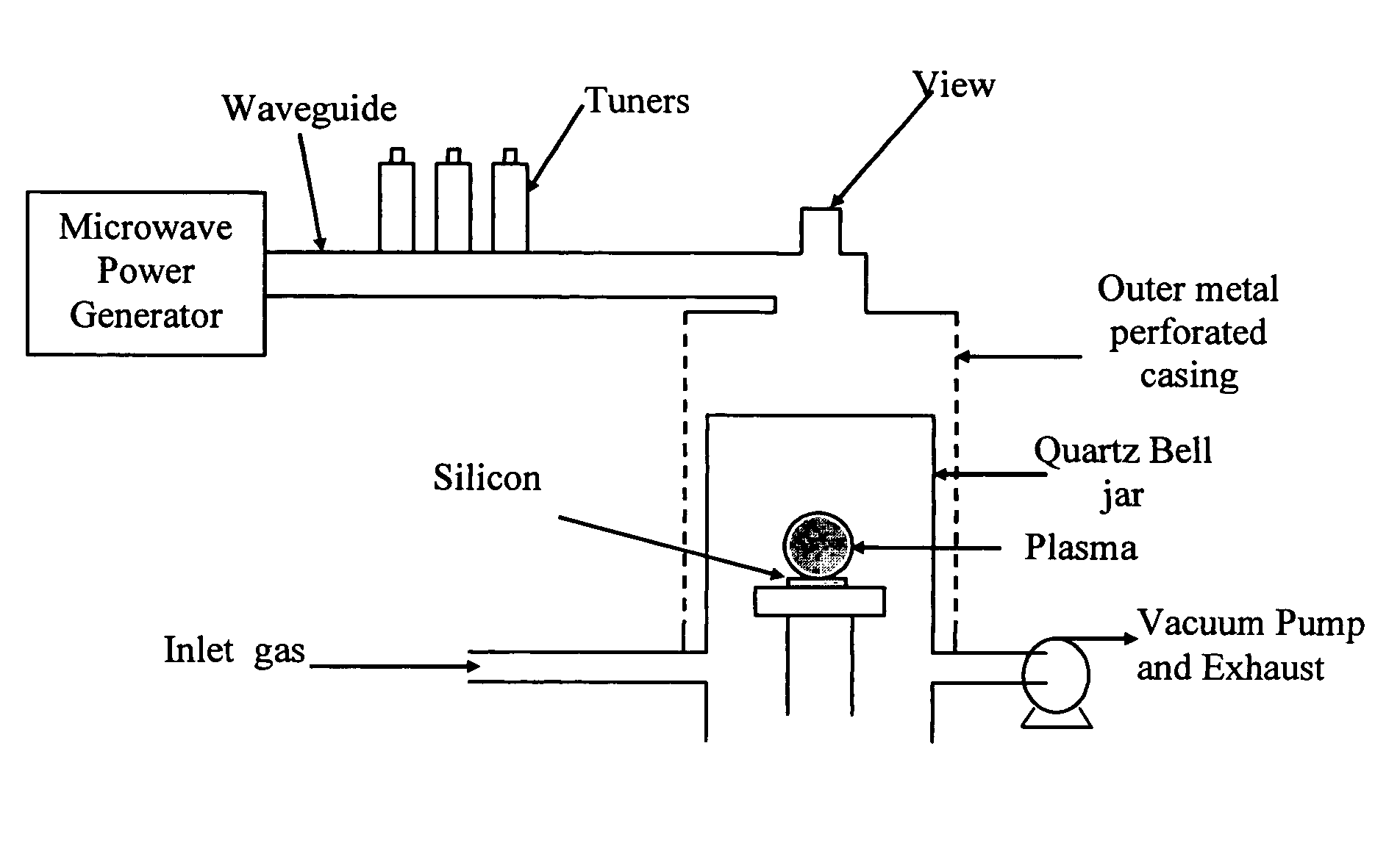
[0073]FIG. 6 shows a schematic of a type of reactor. A silicon substrate (2 cm×2 cm) was prepared by cleaning with a 45% HF solution, thoroughly rinsing in acetone and ultra-sonication. Droplets of gallium metal at 70° C. were applied to form a film with a thickness of approximately 100 microns. The nitrogen flow rate was set to 100 sccm. The pressure in the reactor was set to 30 Torr. Microwaves at 2.45 Ghz were used to ionize the nitrogen gas which served as the carrier gas. The input microwave power was 1000 W. The experiments were done in an ASTeX model 5010 bell jar reactor chamber equipped with an ASTeX model 2115 1500 W microwave power generator. 0.5 sccm of hydrogen were introduced into the nitrogen plasma. The reaction was carried out for six hours. Graphite blocks were used as substrate stage. The quartz bell jar volume was approximately 2000 cc.

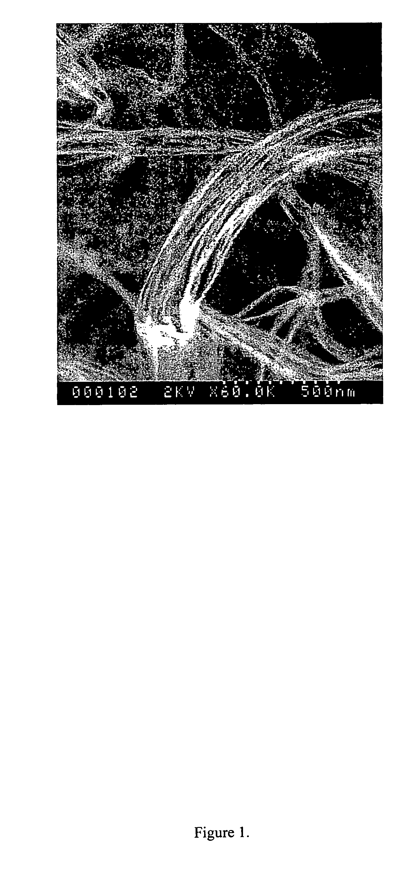
[0074]After the growth experiments, the silicon substrate covered with an ashy mass was observed ...

example 2

Bulk Synthesis of Gallium Oxide Fibers

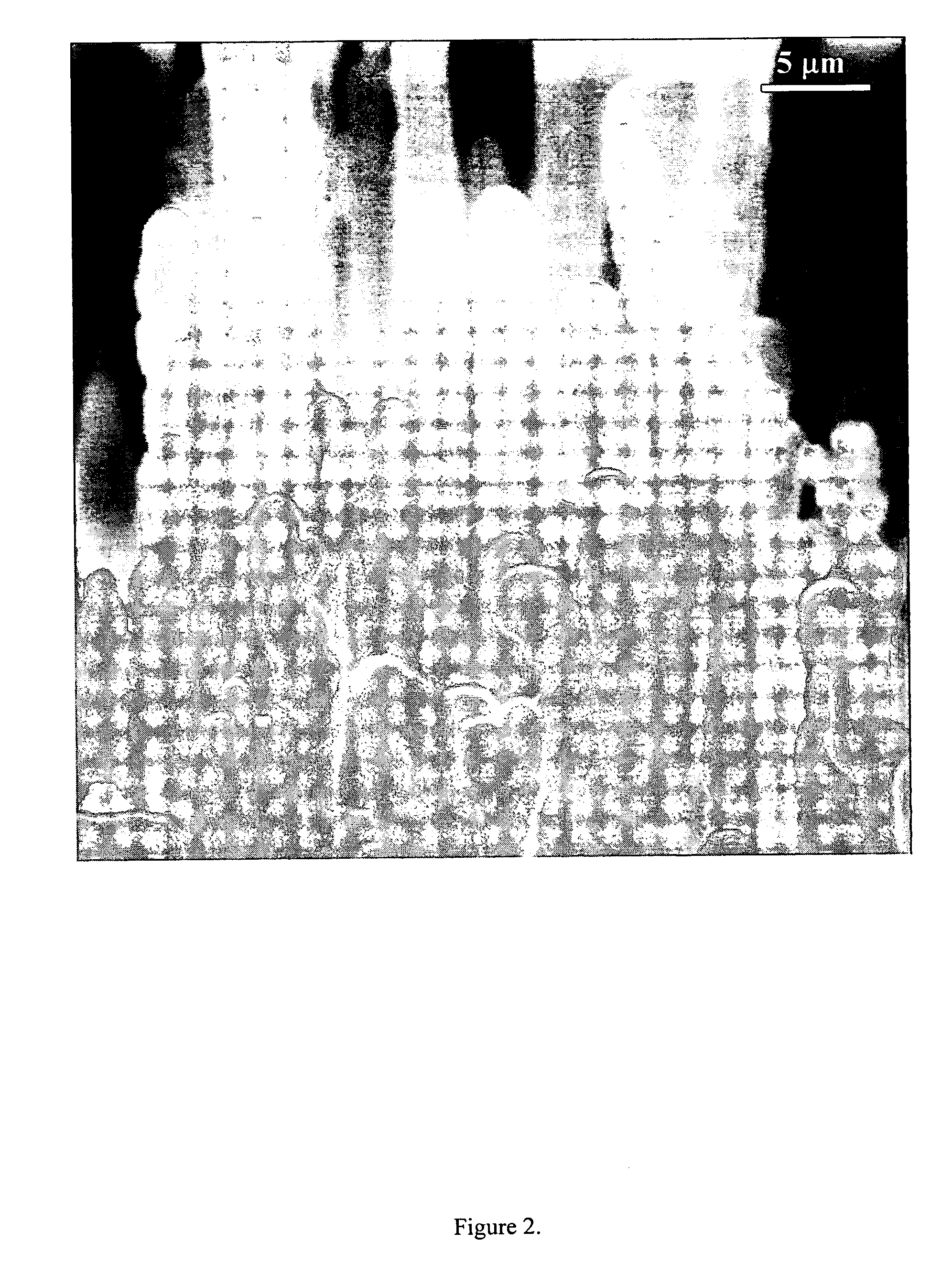
[0092]Gallium oxide fibers can be grown using the above plasma mediated technique. A quartz substrate (2 cm×2 cm) was prepared by ultra-sonication in isopropyl alcohol. Droplets of gallium metal at 70° C. were applied to form a film with a thickness of approximately 100 microns. The hydrogen flow rate was set to 100 sccm. The pressure in the reactor was set to 40 Torr. Microwaves at 2.45 Ghz were used to ionize the hydrogen gas. The input microwave power was 700 W. The experiments were done in an ASTeX model 5010 bell jar reactor chamber equipped with an ASTeX model 2115 1500 W microwave power generator. 0.6 sccm of oxygen were introduced into the hydrogen plasma. The reaction was carried out for four hours. Graphite blocks were used as substrate stage. After the growth experiments, the quartz substrate covered with a whitish mass was observed using a scanning electron microscope (SEM). FIGS. 20 through 25 show micrographs of gallium oxide fiber...

example 3

Synthesis of Carbon Nanofibers

[0096]Carbon nanofibers were grown using the above plasma-mediated technique. A pyrolytic boron nitride substrate (˜1 cm×1 cm) was prepared by ultra-sonication in isopropyl alcohol. The substrate was covered with molten gallium droplets. The hydrogen flow rate was set to 100 sccm. The pressure in the reactor was set to 40 Torr. Microwaves at 2.45 Ghz were used to ionize the hydrogen gas. The input microwave power was 700 W. The experiments were done in an ASTeX model 5010 bell jar reactor chamber equipped with an ASTeX model 2115 1500 W microwave power generator in as shown in FIG. 6. Two (2.0) sccm of methane were introduced into the hydrogen plasma. The reaction was carried out for four hours. Graphite blocks were used as substrate stage. After the growth experiments, the quartz substrate covered with a grey mass was observed using a scanning electron microscope (SEM). FIGS. 30 through 33 show micrographs of carbon nanofibers of various thickness and ...


PUM

PropertyMeasurementUnit
temperatureaaaaaaaaaa
pressureaaaaaaaaaa
thicknessaaaaaaaaaa

Abstract

A process is provided to produce bulk quantities of nanowires in a variety of semiconductor materials. Thin films and droplets of low-melting metals such as gallium, indium, bismuth, and aluminum are used to dissolve and to produce nanowires. The dissolution of solutes can be achieved by using a solid source of solute and low-melting metal, or using a vapor phase source of solute and low-melting metal. The resulting nanowires range in size from 1 nanometer up to 1 micron in diameter and lengths ranging from 1 nanometer to several hundred nanometers or microns. This process does not require the use of metals such as gold and iron in the form of clusters whose size determines the resulting nanowire size. In addition, the process allows for a lower growth temperature, better control over size and size distribution, and better control over the composition and purity of the nanowire produced therefrom.

Description

RELATED APPLICATIONS[0001]This application is a Continuation-In-Part of U.S. application Ser. No. 10 / 664,072, filed on Sep. 16, 2003, now U.S. Pat. No. 7,182,812, claiming priority from U.S. Provisional Application Ser. No. 60 / 411,116, filed on Sep. 16, 2002, and is a Continuation-In-Part of U.S. application Ser. No. 10 / 187,460, now U.S. Pat. No. 7,252,811, filed on Jul. 1, 2002, claiming priority from U.S. Provisional Application Ser. No. 60 / 302,062, filed on Jun. 29, 2001, all of which are incorporated by reference herein.[0002]This application is part of a government project. The research leading to this invention was supported by a Grant Number 9876251 from the National Science Foundation and Air Force Office of Scientific Research. The United States Government retains certain rights in this invention.TECHNICAL FIELD OF THE INVENTION[0003]The invention relates to the field of providing a synthesis technique to grow bulk quantities of semiconductor nanowires, whiskers, and rods a...

Claims


Application Information

Patent Timeline
Patent Type & Authority Patents(United States)
IPC IPC(8): C30B17/00C30B23/00
CPCC30B23/007C30B25/18C30B25/005C30B23/025Y10S977/72Y10S977/762Y10S977/809Y10S977/81Y10S977/825
Inventor SUNKARA, MAHENDRA KUMARSHARMA, SHASHANKCHANDRASEKARAN, HARILI, HONGWEIVADDIRAJU, SREERAM
Owner UNIV OF LOUISVILLE RES FOUND INC
Why Eureka
Try Eureka