
Bulk synthesis of metal and metal based dielectric nanowires

a dielectric nanowire and metal-based technology, applied in the field of bulk synthesis of metal and metal-based dielectric nanowires, can solve the problem of no method for growing freestanding metallic nanowires, and achieve the effect of avoiding laborious and time-consuming processes

Inactive Publication Date: 2010-08-10
UNIV OF LOUISVILLE RES FOUND INC +1
View PDF15 Cites 6 Cited by
  • Summary
  • Abstract
  • Description
  • Claims
  • Application Information

AI Technical Summary

Benefits of technology

[0007]Nanometer scale semiconductor one-dimensional structures such as nanowires are expected to be very important in future high power electronics and opto-electronic device applications. These structures would need metallic interconnects so as to miniaturize the system. Hence it is necessary to develop technology to produce metallic nanowires that can be form hetero-structures directly on the nano-components. It is equally important to be able to form dielectric hetero junctions on semiconductor nanowires to enhance the performance of the device. Furthermore, these metallic nanowires also exhibit photoluminescence in the red-near infrared (IR), region, which also makes it attractive for use as a sensors.
[0012]It is an object of the present invention to provide a process which eliminates the need for quantum sized droplet creation, as is required when transition metals such as gold are used for nanowire synthesis. In principle, the bulk nanowire synthesis technique of the instant invention should work for any material that is immiscible in the gallium solvent. Specifically metal and non-stotiometric metal nitrides (M and MxNy), where M indicates metals such as gold, copper, tungsten, and bismuth.
[0014]It is another object of the present invention to provide a technique to grow freestanding metallic nanowires, which is advantageous in subsequent device fabrication.
[0016]It is another object of the present invention to provide a bulk nanowire synthesis technique forming products having a density of nucleation that is extremely high making it suitable for large scale bulk synthesis.
[0017]It is another object of the present invention to utilize a method using vapor phase precursors, in order to visualize synthesis of metal-semiconductor interfaces and avoid the laborious and time-consuming process of forming contacts to nanoscale devices made of semiconductors.

Problems solved by technology

Currently there exists no method to grow freestanding metallic nanowires.

Method used


Image

  • Bulk synthesis of metal and metal based dielectric nanowires
  • Bulk synthesis of metal and metal based dielectric nanowires
  • Bulk synthesis of metal and metal based dielectric nanowires

Examples


example i

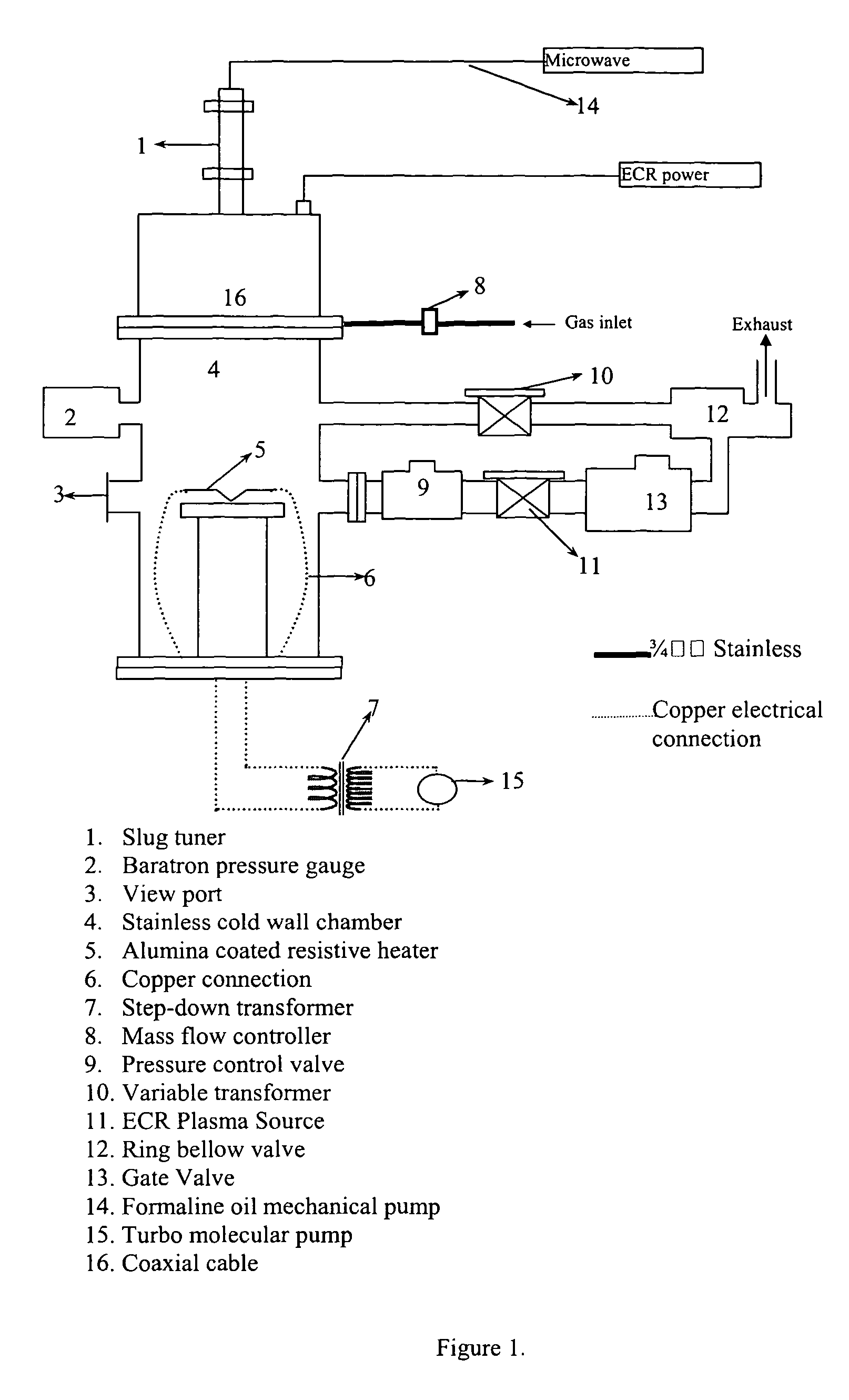
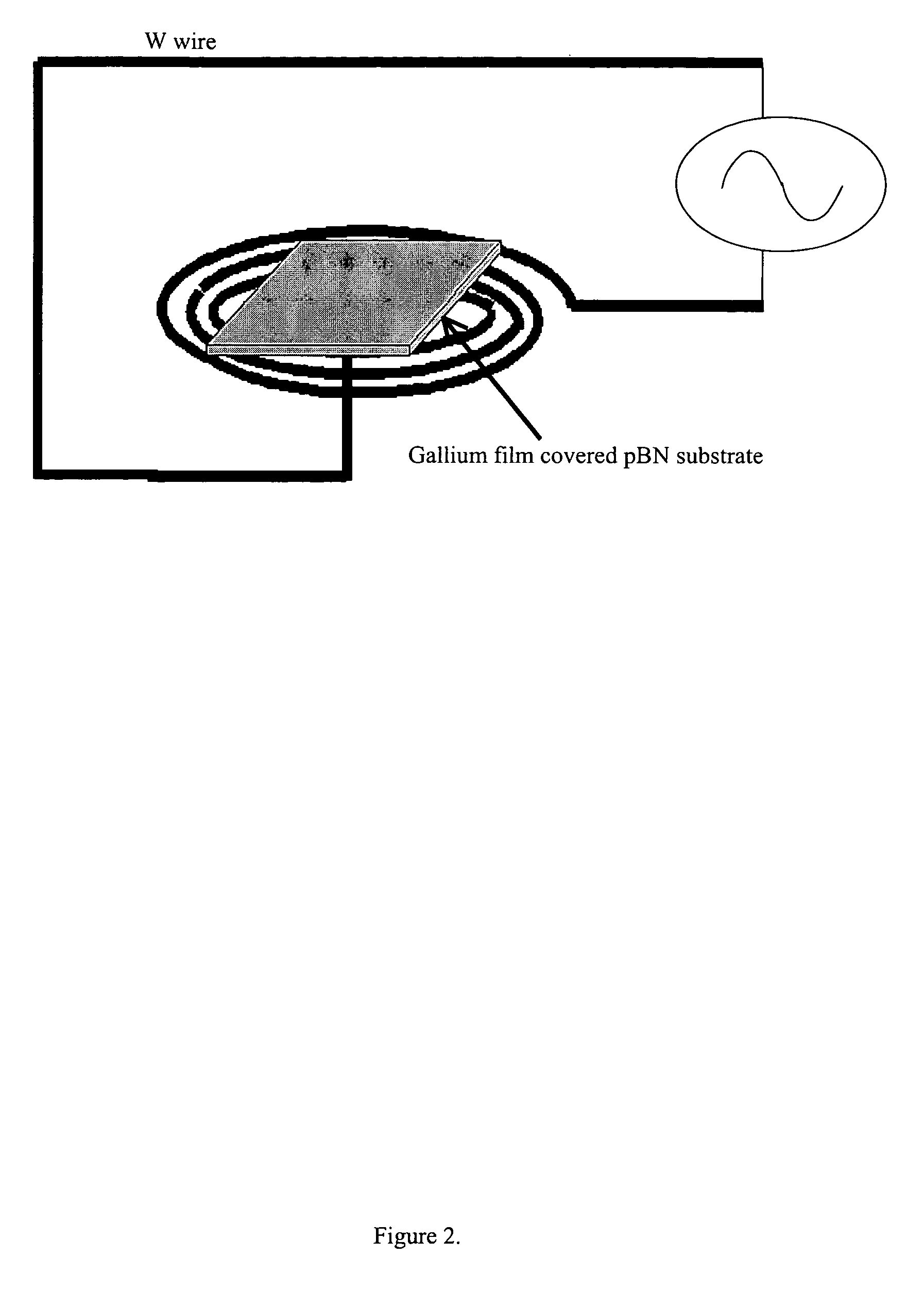
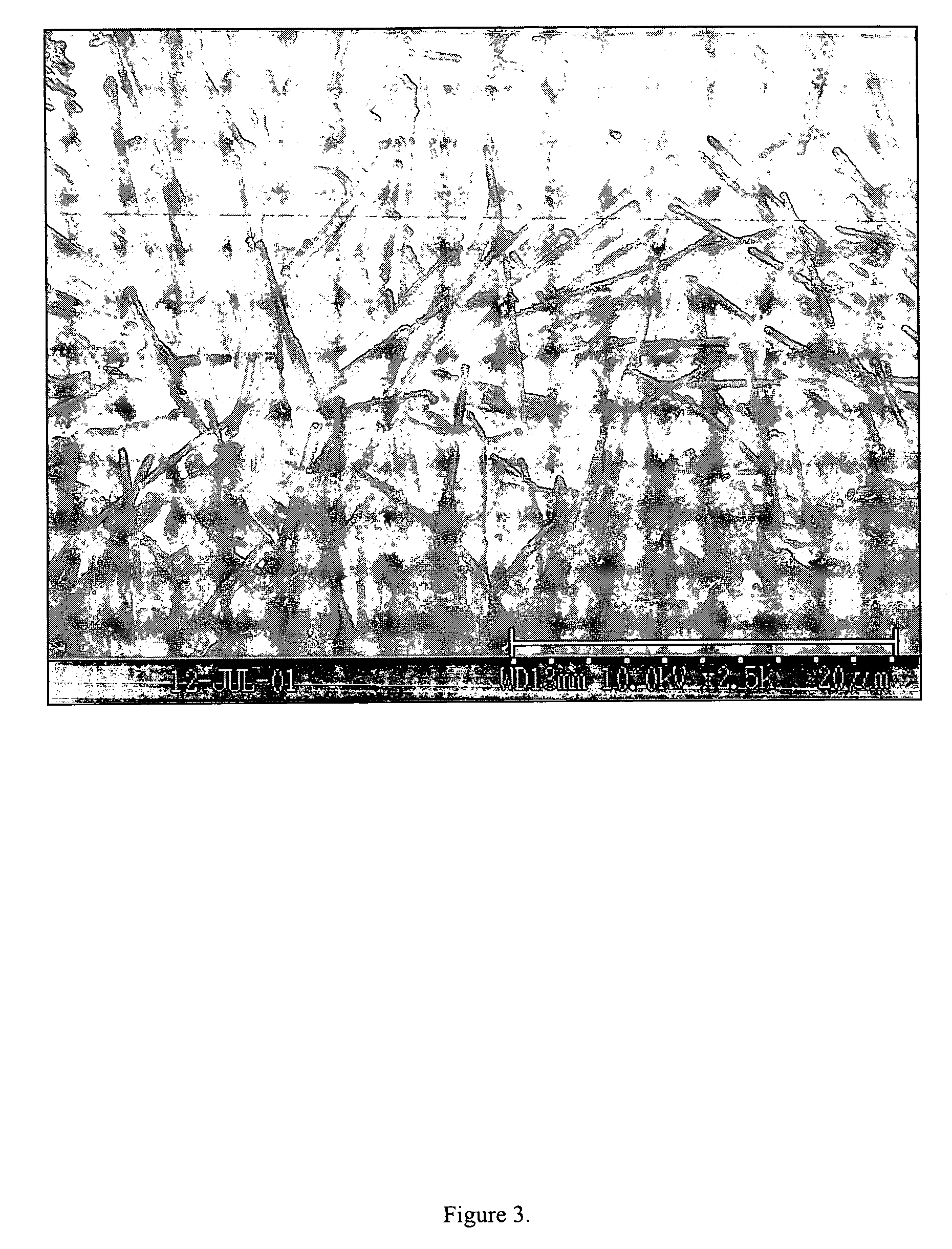
[0034]A flat piece of pyrolytic boron nitride PBN was cleaned with a 45% HF solution and ultra-sonicated acetone before being covered with thin liquid gallium film. This gallium film was resistively heated along with a tungsten wire to a temperature of 900 degrees C. and exposed to an electron cyclotron resonance microwave (ECR-MW) chemical vapor deposition generated nitrogen plasma environment. Nitrogen sputters the tungsten particles onto the gallium film, which subsequently dissolves in liquid gallium. The tungsten (solute) concentration is increased until the gallium (solvent) becomes supersaturated after which, crystallization occurs, and nanowires precipitate from the solvent. It should be noted that the solvent (gallium) metal melt used for the process can be substituted with indium, tin and other low melting metal which serve as catalytic metals.

[0035]As shown in the example, it is an advantage of the instance process is the ability to utilize a template free bulk synthesis ...


PUM

PropertyMeasurementUnit
Pressureaaaaaaaaaa
Lengthaaaaaaaaaa
Lengthaaaaaaaaaa

Abstract

A process of synthesizing metal and metal nitride nanowires, the steps comprising of: forming a catalytic metal (such as gallium, and indium) on a substrate (such as fused silica quartz, pyrolytic boron nitride, alumina, and sapphire), heating the combination in a pressure chamber, adding gaseous reactant and / or solid metal source, applying sufficient microwave energy (or current in hot filament reactor) to activate the metal of interest (such as gold, copper, tungsten, and bismuth) and continuing the process until nanowires of the desired length are formed. The substrate may be fused silica quartz, the catalytic metal a gallium or indium metal, the gaseous reactant is nitrogen and / or hydrogen and the nanowires are tungsten nitride and / or tungsten.

Description

RELATED APPLICATIONS[0001]This application claims priority from Provisional Application Ser. No. 60 / 425,194 filed on Nov. 8, 2002 all of which is incorporated by reference herein.[0002]This application is part of a government project. The research leading to this invention was Supported by a Grant Number F49620-00-1-0310 from Air Force Office of Scientific Research. The United Government retains certain rights in this invention.FIELD OF THE INVENTION[0003]This invention relates to the field of a method of synthesizing free-standing metallic nanowires and dielectric metal nitride nanowires without the use of soft or hard templates.BACKGROUND OF THE INVENTION[0004]Nano-porous templates of alumina are commonly used to grow metallic nanowires. The diameters of the nanowires are controlled only by the size of the pore.[0005]There exists four methods for the growth of GaN nanowires. (1) Confined growth of metal nanowires using carbon nanotubes or nanoporous alumina membranes. In the carbo...

Claims


Application Information

Patent Timeline
IPC IPC(8): C01B21/06B32B15/01C30B11/00C30B15/10C30B35/00H01L21/20H01L21/28H01L21/44
CPCC22C30/00C30B11/002C30B35/002C30B15/10Y10T428/12681Y10T428/12007
Inventor SUNKARA, MAHENDRA KUMARCHANDRASEKARAN, HARILI, HONGWEI
Owner UNIV OF LOUISVILLE RES FOUND INC
Learn More