Photosensitive material, method of manufacturing conductive metal film, conductive metal film and light-transmitting film shielding electromagnetic wave for plasma display panel

a technology of shielding electromagnetic wave and photosensitive materials, which is applied in the direction of photosensitive materials, metallic image processing, instruments, etc., can solve the problems of health problems of operators of facilities, difficulty in recognizing characters displayed on the screen, and screen darkening, so as to reduce the resistance value

Inactive Publication Date: 2010-11-09
FUJIFILM CORP
View PDF27 Cites 10 Cited by
  • Summary
  • Abstract
  • Description
  • Claims
  • Application Information

AI Technical Summary

Benefits of technology

[0040]According to the invention, when the swelling rate of an emulsion layer is set at 150% or more, a photosensitive material capable of obtaining a conductive metal film of which electric resistance value is reduced can be provided. Furthermore, according to the invention, a light-transmitting film shielding conductive electromagnetic wave high in the electromagnetic wave shielding property and excellent in the plating velocity and the uniformity can be provided.

Problems solved by technology

It is pointed out that the EMI causes, in addition to causing malfunction and disturbance of the electric and electronic facilities, health problem to operators of the facilities.
Accordingly, since, in all of the above-mentioned methods, in many cases, front surfaces of the displays are obscured, these are improper as a method of shielding against electromagnetic wave.
However, there is a disadvantage in that since the shielding material is large in a mesh line width, when it is used to shield a display screen, a screen becomes darker and characters displayed on the screen are difficult to recognize.(2) Electroless-plating Processed Mesh
However, since a line width of the printed catalyst is such large as substantially 60 μm, the method is not suitable for use in a display that requires a relatively small line width and a dense pattern.
However, the visible light-transmittance of the conductive film, being 72%, is insufficient in the transparency.
In addition, since extremely expensive palladium must be used as the electroless plating catalyst, most part of which is removed after the exposure, this method also suffers from a problem of production cost.(3) Mesh Etched by Use of Photolithography
However, this method suffers from problems of a troublesome and complicated production process and thus high production cost.
Furthermore, it is known that there is a problem in that, since the etching process is used, the width of the intersectional points in the grid pattern becomes thicker than that of the straight-line portions.
Accordingly, there is a problem in that opaque physical development nuclei remain on an exposed portion where a metallic silver film is not formed, and thereby light transmission is degraded.
The aforementioned problem is serious particularly in a case when the metal pattern material is used as a light-transmitting material shielding electromagnetic wave for a display such as a CRT and PDP.
Furthermore, it is also difficult to obtain high electric conductivity by use of those methods, and attempts of obtaining a thick silver film for higher electric conductivity are accompanied by a problem of degradation of the transparency.
Accordingly, even when the aforementioned silver salt diffusion transfer process is used as it is, the light-transmitting material shielding electromagnetic wave excellent in the light transmission and electric conductivity and thus suitable for shielding electromagnetic waves from an image display screen of an electronic display facility cannot be obtained.
Still furthermore, when, without using the silver salt diffusion transfer process, the electric conductivity is imparted by using a commercially available usual negative film and by subjecting to development, physical development and plating processes, obtainable conductivity and optical transparency are insufficient for use as a light-transmitting material shielding electromagnetic wave for CRTs or PDPs.
However, since there is a limit, a technology of further reducing the electric resistance value of the developed silver is in demand.

Method used


Image

  • Photosensitive material, method of manufacturing conductive metal film, conductive metal film and light-transmitting film shielding electromagnetic wave for plasma display panel
  • Photosensitive material, method of manufacturing conductive metal film, conductive metal film and light-transmitting film shielding electromagnetic wave for plasma display panel
  • Photosensitive material, method of manufacturing conductive metal film, conductive metal film and light-transmitting film shielding electromagnetic wave for plasma display panel

Examples


example 1

Preparation of Emulsion A

[0220]First Solution:

[0221]

Water750mlGelatin20gSodium chloride1.6g1,3-dimethylimidazolidine-2-thion20mgSodium benzene thiosulfonate10mgCitric acid0.7mg[0222]Second Solution:

[0223]

Water300 mlSilver nitrate150 g[0224]Third Solution:

[0225]

Water300mlSodium chloride38gPotassium bromide32gPotassium hexachloroiridate (III)5ml(0.005% KCl 20% aqueous solution)Ammonium hexachlororhodate7ml(0.001% NaCl 20% aqueous solution)

[0226]A potassium hexachloroiridate (III) (0.005% KCl 20% aqueous solution) and an ammonium hexachlororhodate (0.001% NaCl 20% aqueous solution) that are used in the third solution were prepared by dissolving powders thereof, respectively, in a 20% KCl aqueous solution and a 20% NaCl aqueous solution, followed by heating at 40° C. for 120 min.

[0227]To the first solution kept at 38° C. and pH 4.5, amounts equivalent to 90% of the respective second and third solutions were simultaneously added under stirring over 20 min, and thereby nuclei of 0.15 μm w...

example 2

Preparation of Samples 2-1 to 2-4

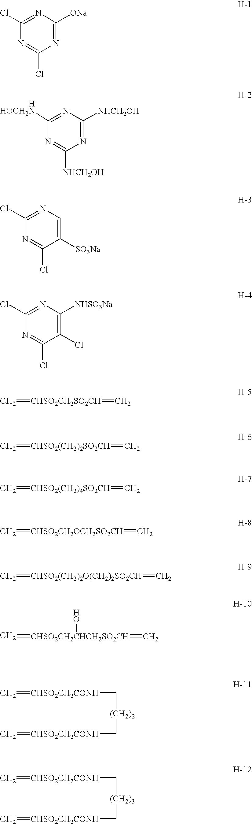
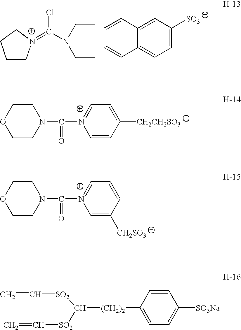
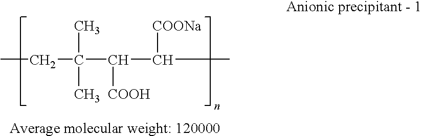
[0292]Except that, in the sample 1-1 according to the example 1, to the emulsion layer, 90 mg / m2 of 2,4-dichloro-6-hydroxy-1,3,5-triazine sodium salt was added, and, to the gelatin, 15% by weight of colloidal silica having a particle diameter of 10 μm, 100 mg / m2 of aqueous latex (aqL-6), 150 mg / m2 of polyethyl acrylate latex, 150 mg / m2 of a latex copolymer of methyl acrylate, 2-acrylamide-2-methyl propane sulfonate sodium salt and 2-acetoxyethyl methacrylate (weight ratio 88:5:7) and 150 mg / m2 of core-shell type latex (core: styrene / butadiene copolymer (weight ratio 37 / 63), shell: styrene / 2-acetoxyethyl acrylate (weight ratio 84 / 16), and core / shell ratio=50 / 50) were added, utterly similarly to the sample 1-1, a sample 2-1 was obtained.

[0293]In the sample 2-1, only an amount of coated silver, an amount of coated gelatin and an amount of coated (Cpd-7) were altered as shown in Table 2 and thereby samples 2-2 to 2-4 were obtained. Here, when the weight ...

example 3

[0297]Except that, in the samples 1-1 to 1-4 prepared in the example 1, a spectral sensitizing dye SD-1 was altered to a spectral sensitizing dye SD-2, the Cpd-14 was altered to Cpd-YF below, and a back layer was not coated, similarly to the samples 1-1 to 1-4, samples 3-1 to 3-4 were prepared. Furthermore, except that in the samples 2-1 to 2-4 prepared in the example 2, the spectral sensitizing dye SD-1 was altered to the spectral sensitizing dye SD-2, the Cpd-14 was altered to Cpd-YF below, and a back layer was not coated, similarly to the samples 2-1 to 2-4, samples 3-5 to 3-8 were prepared. Coating amounts of the SD-2 and Cpd-YF were set to amounts (mole m2) same as that of SD-1 and Cpd-14.

[0298]The obtained samples were subjected to exposure by use of a contact printer with a high-pressure mercury lamp as a light source through a mesh-like photomask having a fine line width of 10 μm and a grid separation of 300 μm, followed by applying a development process and a plating proces...


PUM

PropertyMeasurementUnit
weight ratioaaaaaaaaaa
transparencyaaaaaaaaaa

Abstract

A photosensitive material includes a support and an emulsion layer containing a silver salt emulsion, the photosensitive material is capable of forming a conductive metal film by exposing and developing the emulsion layer, wherein the emulsion layer has a swelling rate of 150% or more.

Description

TECHNICAL FIELD[0001]The invention relates to a photosensitive material that can form a conductive metal film that can shield an electromagnetic wave generated from a front surface of a display such as a CRT (Cathode Ray Tube), a PDP (Plasma Display Panel), a liquid crystal panel, an EL (electroluminescent) panel, a FED (Field Emission Display) or the like, a microwave oven, an electronics device, a printed wiring board or the like and can form a conductive metal film having transparency. Furthermore, the invention relates to a manufacturing method of a conductive metal film, a conductive metal film and a light-transmitting film shielding electromagnetic wave for plasma display panels.BACKGROUND ART[0002]Recently, with an increase in the use of various kinds of electric facilities and applied electronic facilities, an EMI (Electro-Magnetic Interference) is in a rapid increase. It is pointed out that the EMI causes, in addition to causing malfunction and disturbance of the electric a...

Claims


Application Information

Patent Timeline
Patent Type & Authority Patents(United States)
IPC IPC(8): G03C1/00G03C1/005G03F7/00G03F7/40
CPCG03C1/30G03C5/58Y10T428/24917G03C2200/27G03C2007/3025G03C2001/0476
Inventor NAKAHIRA, SHINICHI
Owner FUJIFILM CORP
Why Eureka
Try Eureka