

Transparent, electrically conductive layer, a process for producing the layer and its use
a technology of electrical conductive layer and transparent layer, which is applied in the direction of organic semiconductor devices, group 3/13 element organic compounds, synthetic resin layered products, etc., can solve the problems of high cost, complex, and low layer transmission efficiency
- Summary
- Abstract
- Description
- Claims
- Application Information
AI Technical Summary
Benefits of technology
Problems solved by technology
Method used
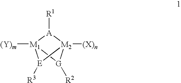
Image


Examples
examples
General Techniques
[0117]All syntheses involving organometallic compounds were effected, owing to their high air and moisture sensitivity, in a protective gas atmosphere composed of nitrogen which was available through evaporation of liquid nitrogen (Messer Griesheim). All reactions were effected with the aid of standard Schlenk techniques or in a glovebox.
[0118]Before utilization under reduced pressure, the glass apparatus used was baked out with a naked flame and, after cooling, filled with nitrogen and evacuated three times. Only after this operation was the filling of chemicals commenced. Liquid substances were transferred by means of syringes and cannula which were stored in a drying cabinet and flushed repeatedly with nitrogen before use.
[0119]In the syntheses, only anhydrous chemicals were used. The solvents used were dried by standard methods: tetrahydrofuran, diethyl ether, toluene, n-pentane and n-hexane were absoluted with sodium and benzophenone in the protective atmosphe...
PUM
| Property | Measurement | Unit |
|---|---|---|
| thickness | aaaaa | aaaaa |
| transparent | aaaaa | aaaaa |
| thickness | aaaaa | aaaaa |
Abstract
Description
Claims
Application Information