

Bond pad with integrated transient over-voltage protection
a bond pad and transient protection technology, applied in the direction of emergency protective circuit arrangement, emergency protection circuit arrangement, etc., can solve the problem of limiting the reliability design factor, esd-induced damage is a limiting factor, and high-voltage ics are increasingly susceptible to damage, etc., to achieve rapid triggering, increase conductivity modulation, and small footprint
- Summary
- Abstract
- Description
- Claims
- Application Information
AI Technical Summary
Benefits of technology
Problems solved by technology
Method used
Image

Examples
Embodiment Construction
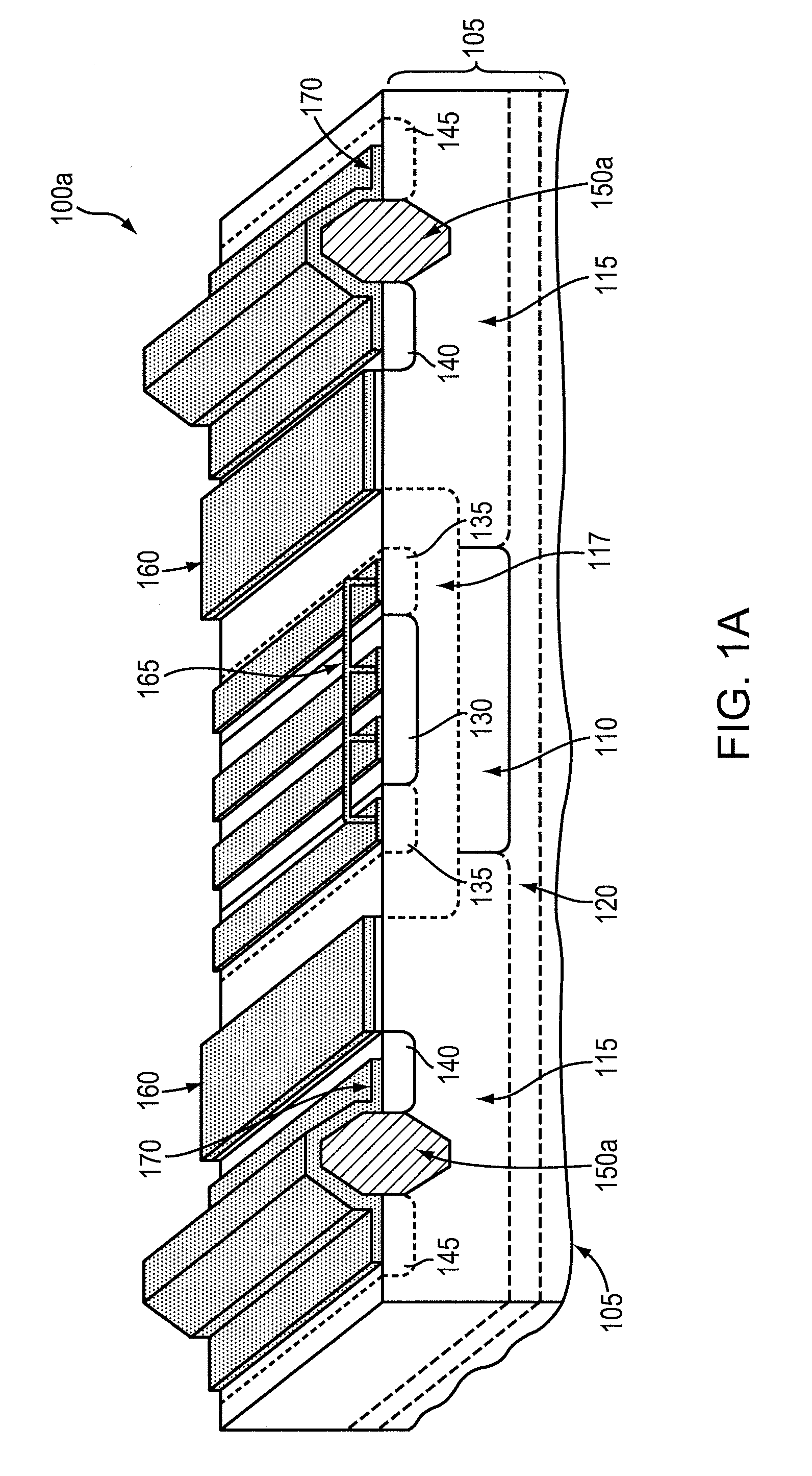
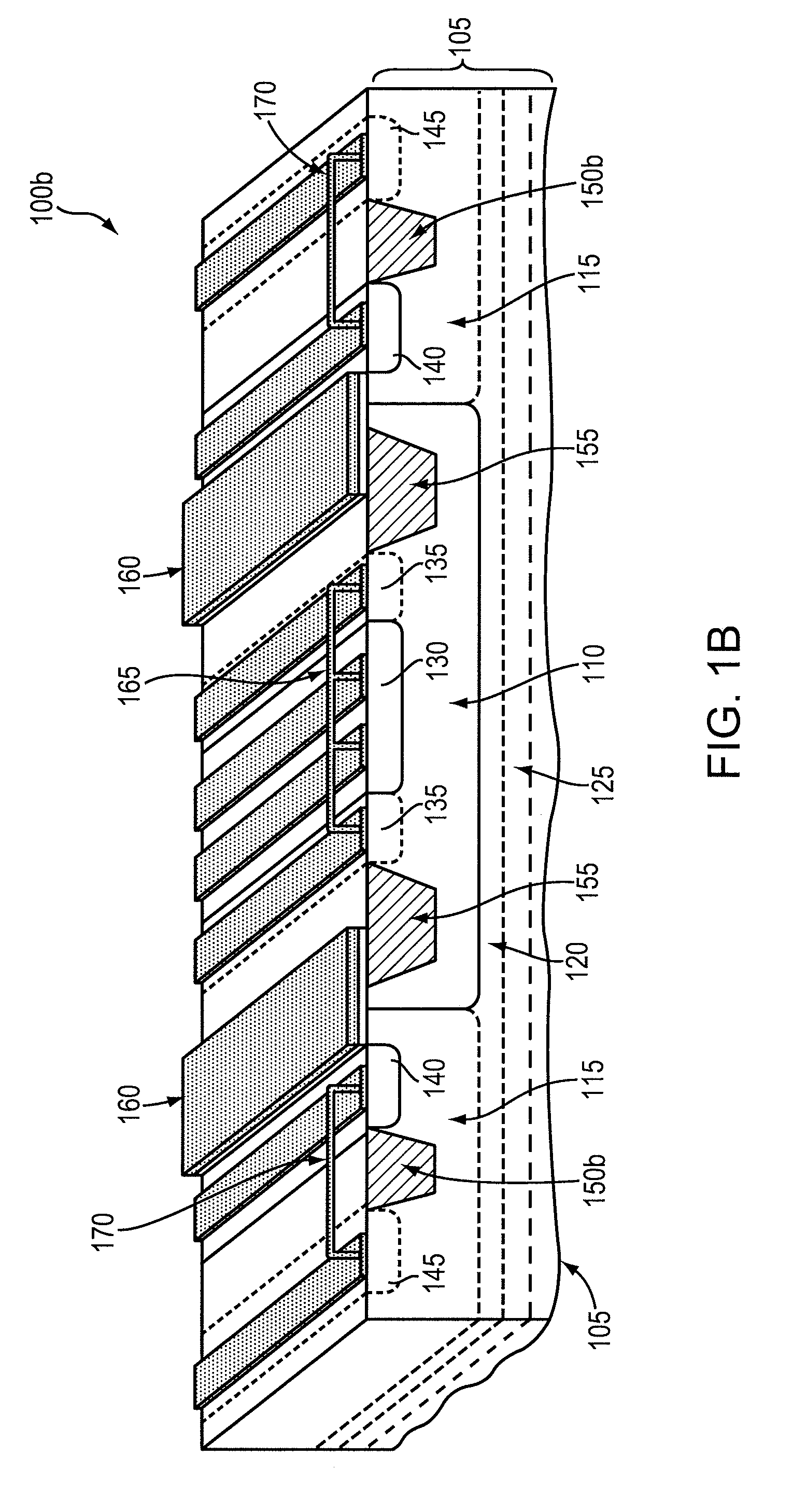
[0036]The present invention provides, in various embodiments, transient over-voltage clamp devices with improved protection characteristics. FIGS. 1A-1C illustrate exemplary planar MOS embodiments 100a, 100b, and 100c. These and other embodiments of the invention can be produced using standard semiconductor device fabrication techniques, including silicon epitaxy, layer deposition and patterning, doping by ion implantation or diffusion, and subsequent metal interconnecting.
[0037]Each of the exemplary structures 100a, 100b, 100c comprises a semiconductor substrate 105 (e.g., silicon) and, embedded therein, doped deep-well regions 110, 115 of alternating conductivity types. For example, a central well 110 may be doped with a negative dopant (e.g., group V atoms such as phosphorus or arsenic), and the adjacent wells 115 to both sides may, accordingly, be doped with a positive dopant (e.g., group III atoms such as boron). Between the deep-well regions 110, 115, a metallurgical junction ...
PUM
 Abstract
Description
Claims
Application Information