Coatings, and methods and devices for the manufacture thereof

a technology of coatings and metal interconnects, applied in the direction of chemical vapor deposition coatings, nanotechnology, coatings, etc., can solve the problems of increasing interconnect problems, limiting the performance of high-speed logic chips, and the small size of wires became an issue, so as to improve the adhesion of activated intermediates, increase the deposition rate of different activated components, and increase the gas or vapor stream

Active Publication Date: 2012-07-31
ASM INTERNATIONAL
View PDF11 Cites 6 Cited by
  • Summary
  • Abstract
  • Description
  • Claims
  • Application Information

AI Technical Summary

Benefits of technology

[0117]The ratio of inorganic to organic components, the density of the low dielectric material that is manufactured in this way and the amount of nanoparticles present can be fully controlled. In this way, many different specific properties can be imparted to the material. Also, to the different plasmas additives can be added, enabling specific properties to be imparted to a coating according to the invention.
[0118]Any substrate is suitable to be clad with a coating according to the invention provided that the activated intermediates can adhere to it. Suitable substrates for applying a coating according to the present invention are substrates generally used in the semiconductor industry, and may for instance include plastic, metal, glass and ceramics.
[0119]The thickness of the coating can be adjusted by varying the vapor deposition time (the period in which the substrate is exposed to the chemical vapor phase). Thicker coatings are achieved after longer vapor deposition times. Optionally, the deposition rate of the different activated components can be increased by supplying more energy to the plasmas or by increasing the gas or vapor stream through the device.
[0120]The substrate can optionally be cleaned or otherwise treated to improve the adhesion of activated intermediates, and hence the entire coating. Such treatment methods are known in the art and comprise treatment with, for instance, HF, NH4OH or H2SO4, or with the aid of a plasma according to methods known for that purpose.

Problems solved by technology

As the dimensions of integrated circuit (IC) devices scale to smaller feature sizes, the resistance-capacitance (RC) delay of the metal interconnect is limiting the performance of high speed logic chips [1, 2].
As scaling went into the submicron range, the small size of the wires became an issue.
But despite the presence of a number of candidate materials with dielectric constants k in the range of 2-3 [3], the interconnect issues are becoming increasingly problematic.
But despite the fact that highly porous materials with low dielectric constants have been obtained, their susceptibility and weakness make the low-k materials produced by sol-gel processes presently unsuitable for implementation into semiconductor processing.
Various problems are associated with porous SiO2 layers.
The porosity of these materials introduces technical problems when they are implemented into copper based interconnect integrated circuits (ICs).
Porous materials are mechanically weak compared to dense materials, and porous materials are susceptible to damage during subsequent processing.
In addition, porous materials are sensitive to wet and dry cleaning chemicals and they hold volatile compounds that when liberated contaminate subsequent processing steps [26].
However, gas phase deposition techniques typically produce dense deposits.
Unfortunately, conventional gas phase technologies offer insufficient control over the deposition chemistry and therefore less control over film structure and consequently polarizability.
A drawback of the method of Grill et al. is that a post deposition curing is required, making the process more complex.

Method used


Image

  • Coatings, and methods and devices for the manufacture thereof
  • Coatings, and methods and devices for the manufacture thereof
  • Coatings, and methods and devices for the manufacture thereof

Examples


example 1

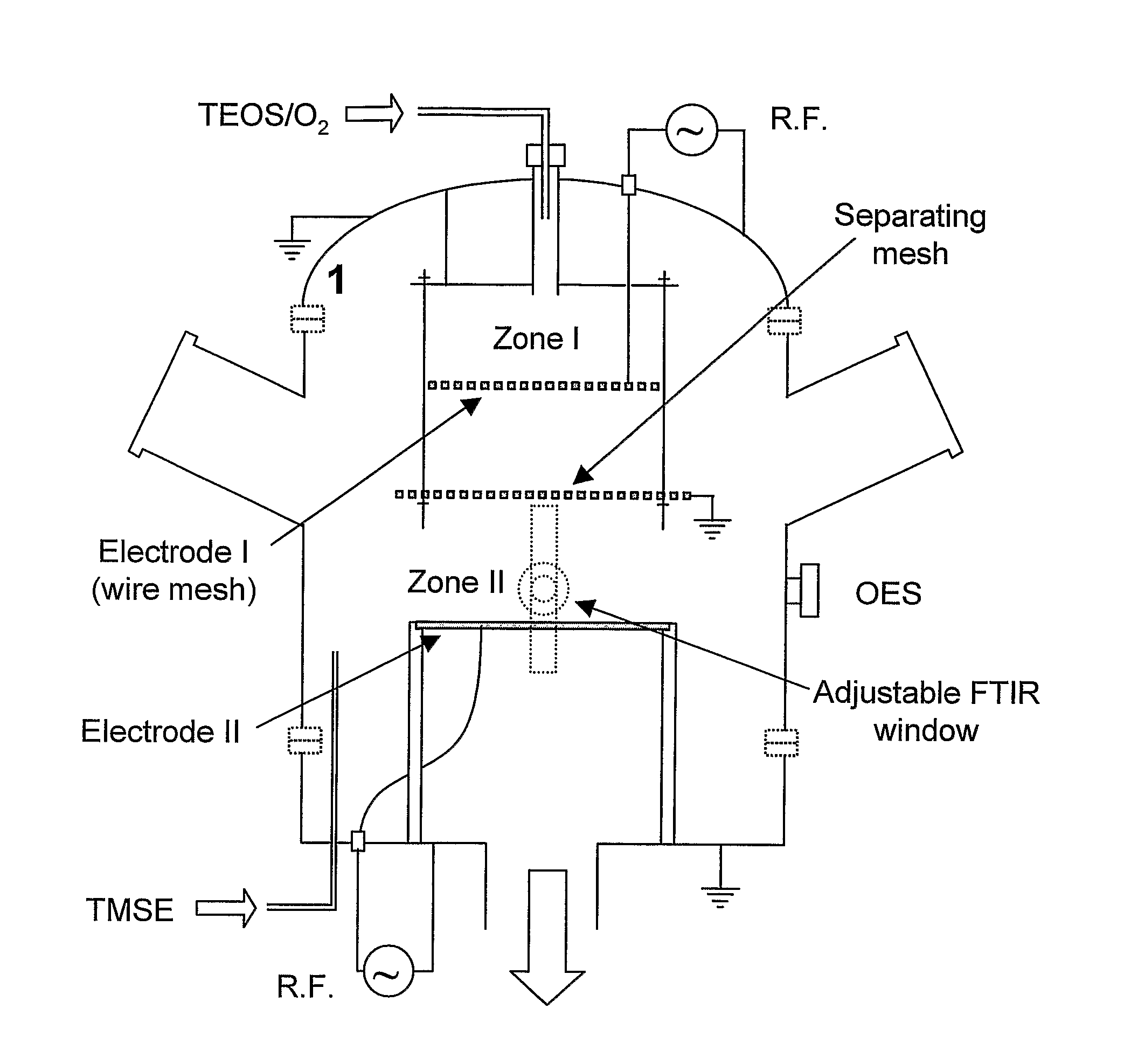
[0121]In this Example a dual capacitive plasma reactor is used in combination with a process to synthesize nanoporous particles and simultaneously incorporate them into a silicone layer. The nanoporosity of these particles is used to introduce controlled porosity into the silicone layers with the aim of producing low-k layers. Nanocomposite layers exhibiting dielectric constants of 1.82-1.86 (1.82±0.02 ) have been demonstrated, compared to 3.05 for similar layers without particle incorporation.

Reactor

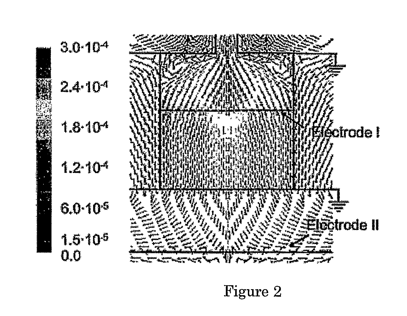
[0122]The reactor design comprises two capacitively coupled plasma systems each connected to a power of 1 kW at 13.56 MHz supplied through matching networks (FIG. 1). The plasmas may or may not be pulsed, preferably they are pulsed. The precursors and gasses, e.g. TEOS and oxygen, for particle synthesis, may be fed into Zone I, e.g. through the top inlet indicated, where they are activated by the plasma formed between the radio frequency (r.f.) electrode mesh (i.e. the mesh acting as el...

example 2

[0157]In this Example the synthesis, monitoring and characterisation of nanoparticles and their incorporation into low dielectric constant layers using the dual capacitive plasma reactor is described in more detail.

Introduction

[0158]In deposition systems used in the semiconductor and micro electronic industries, particle production is an undesirable by-product of some plasma processing steps. Device failure as a result of dust contamination is a familiar issue and has prompted research into particle formation and transport mechanisms in the hope that it might be avoided. A prominent area of literature regarding particle contamination deals with silane chemistries due to its widespread application in industrial processes. Although particles have been observed in TEOS and HMDSO plasma discharges, very little has been done in elucidating the mechanism by which they are formed. This is perhaps partly due to the added complexity of these gas mixtures brought on with the addition of the c...


PUM

PropertyMeasurementUnit
dielectric constantsaaaaaaaaaa
dielectric constantaaaaaaaaaa

Abstract

The present invention describes a method for manufacturing a low dielectric constant coating, which coating comprises an inorganic and an organic component, wherein precursors for these components are activated in at least two plasma sources for plasma activated deposition of a chemical vapor phase and wherein said activated precursors are combined before they are deposited from the chemical vapor phase on the substrate to form the coating, characterized in that said inorganic component comprises porous nanoparticles. The invention also describes a device for the manufacture of a low dielectric constant coating.

Description

[0001]This application is a §371 national phase filing of PCT / NL2005 / 000279 filed Apr. 14, 2005, and claims priority to European application No. 04 076 150.4 filed Apr. 14, 2004.BACKGROUND OF THE INVENTION[0002]The invention relates to methods for the manufacture of coatings having low dielectric constants and to devices for the manufacture thereof.[0003]As the dimensions of integrated circuit (IC) devices scale to smaller feature sizes, the resistance-capacitance (RC) delay of the metal interconnect is limiting the performance of high speed logic chips [1, 2]. Up until a decade ago, the resistance caused by interconnects in microprocessors was less than the switching time of transistors, so interconnect resistance was not a factor in microprocessor design. As scaling went into the submicron range, the small size of the wires became an issue. As wires get thinner, their resistance increases. Chip designers responded by switching from aluminum to copper as a material for the intercon...

Claims


Application Information

Patent Timeline
Patent Type & Authority Patents(United States)
IPC IPC(8): C23C16/00C23F1/00H01L21/306C23C16/50B05D7/24C09D5/24C23C16/30C23C16/40C23C16/452C23C16/509H01J37/32H01L21/312H01L21/316
CPCB05D1/60B05D2601/20B82Y30/00C09D5/24C23C16/401C23C16/509H01L21/02126H01L21/02203H01L21/02274H01L21/0228H01L21/31695H01L21/312H01L21/31612
Inventor ALCOTT, GREGORY ROBERTCREATORE, MARIADRIANALINDEN, JOANNES LEONARDSANDEN, MAURITIUS CORNELIS MARIA VAN DE
Owner ASM INTERNATIONAL
Why Eureka
Try Eureka