[0003]The present invention relates to a transistor that can further reduce feature size and improve transistor performance without discarding the investment in
integrated circuit fabrication processes. Significant improvements in transistor and
integrated circuit performance can be obtained with this device by building on the capabilities of
silicon fabrication foundries rather than requiring a shift in manufacturing infrastructure as might be required by other technologies.
[0005]As noted previously, scaling has been very productive as a strategy to improve integrated
circuit performance. Scaling feature sizes down with 90-nm process technology that is starting commercial production, will produce transistors with 50-nm gates and 1.2-nm thick gate oxides, which are only 5 atomic
layers thick. Much of the effort to improve device performance focuses on reducing the leakage current due to short channel effects
and gate leakage current and increase speed by improving mobility or
transconductance.
[0006]Efforts to improve the
transconductance in field-effect transistors range from the use of strained-
silicon layers with high mobility in
silicon integrated circuits to modulation-doped
quantum well
high electron mobility transistors (HEMTs) in III-V materials. The use of strain has been shown to improve the mobility of silicon materials. In III-V materials, a
quantum well with lower energy gap material and low
doping is placed into the channel and carriers fall into the well and are conducted in a two dimensional
electron gas with low
impurity scattering. The improvements obtained from these approaches result in increased mobility,
transconductance gm, and hence improved gm / C ratios, where C is the transistor input
capacitance. Higher gm / C translates into improved operation at high frequencies. HEMTs are currently in commercial production and strained-layer silicon will soon be in production.
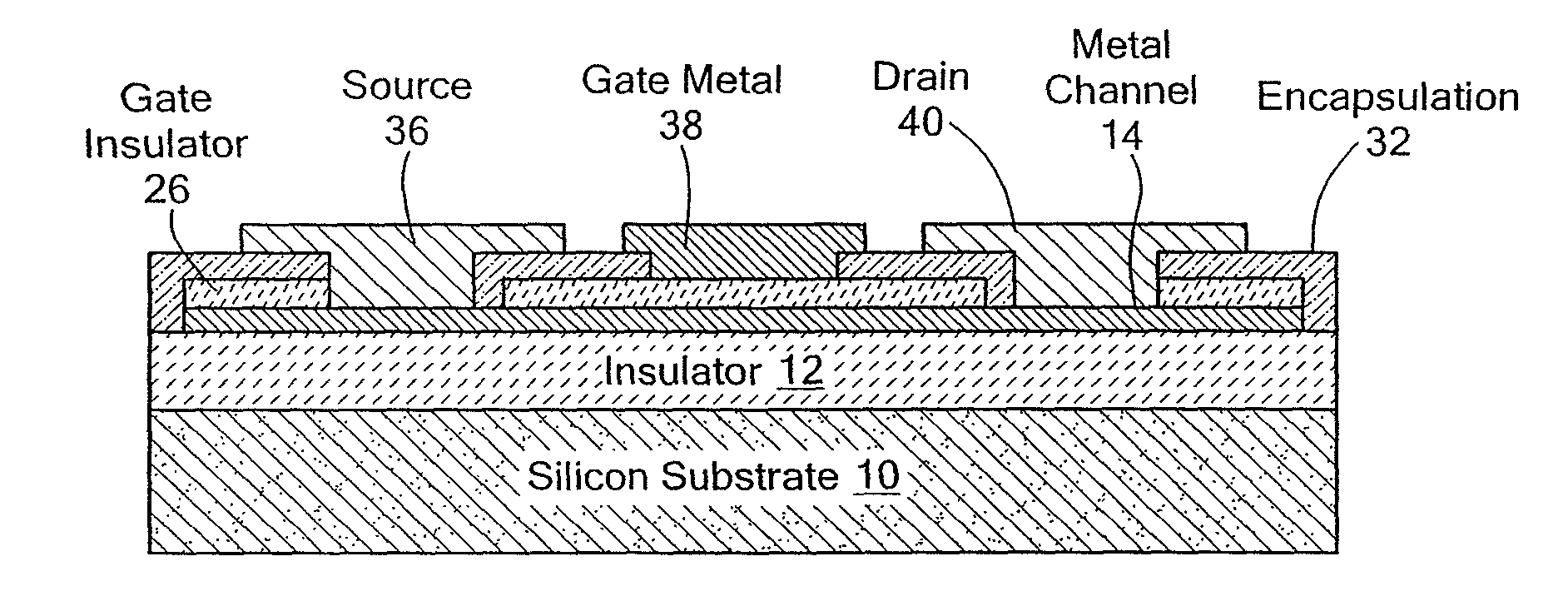
[0007]The present invention pertains to devices referred to herein as metal transistors. These devices are
field effect devices with a
thin metal channel. Advantages of the metal transistor include higher transconductance and improved high-speed operation. The
high conductivity of the metal channel eliminates punch through effects even at gate lengths of 10 nm or less. In addition, the
high conductivity of metal-to-metal source and drain contacts enables such contacts to be made in a small area relative to metal-
semiconductor ohmic contacts. The
thin metal channel makes three-dimensional effects less important.
Metal transistors can therefore be expected to scale to smaller sizes than silicon devices. Furthermore, metal transistors not only can be made on silicon at densities common to silicon integrated circuits, but can also be integrated onto a variety of substrates, including optoelectronic and / or electro-optic materials.
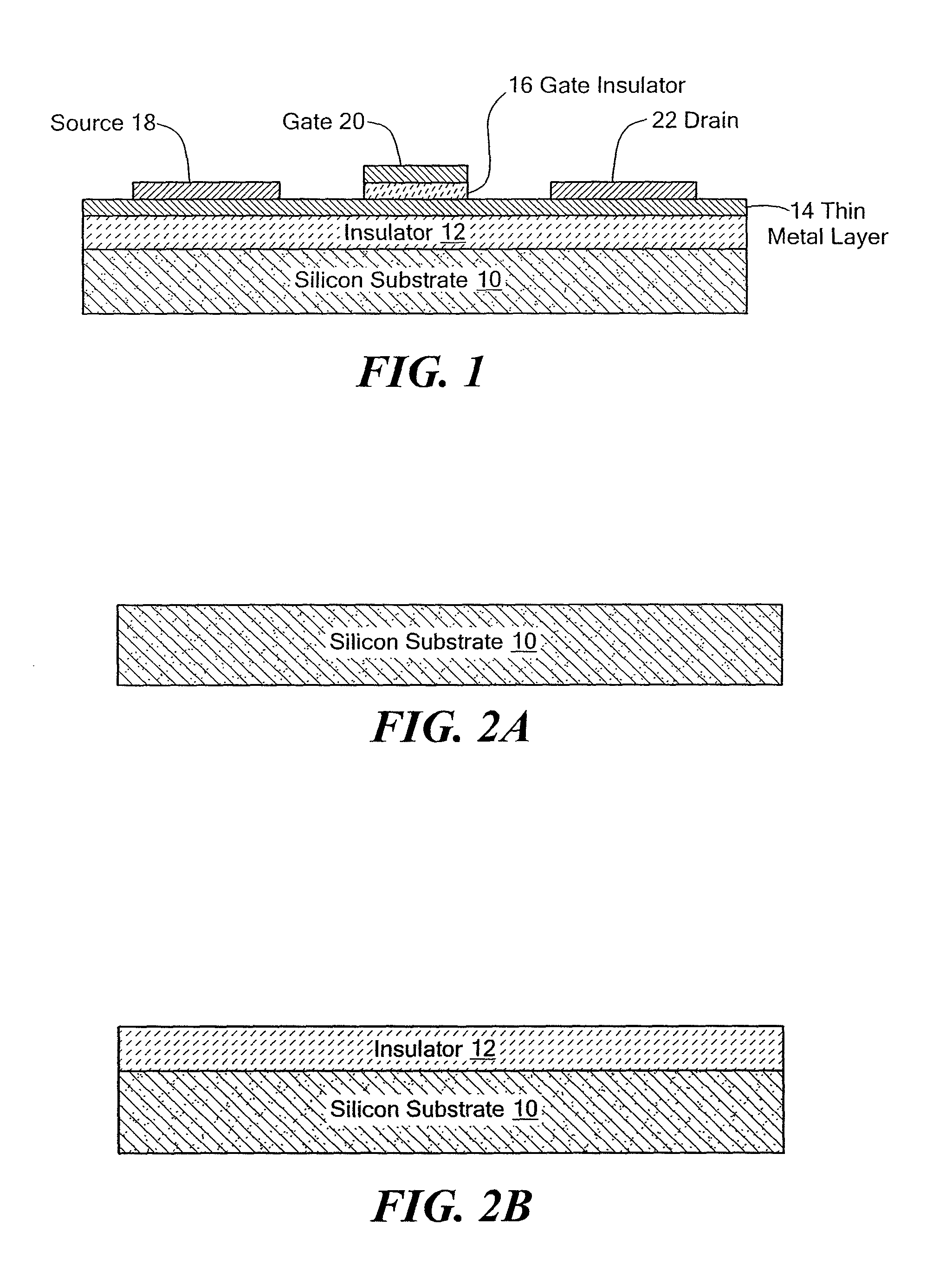
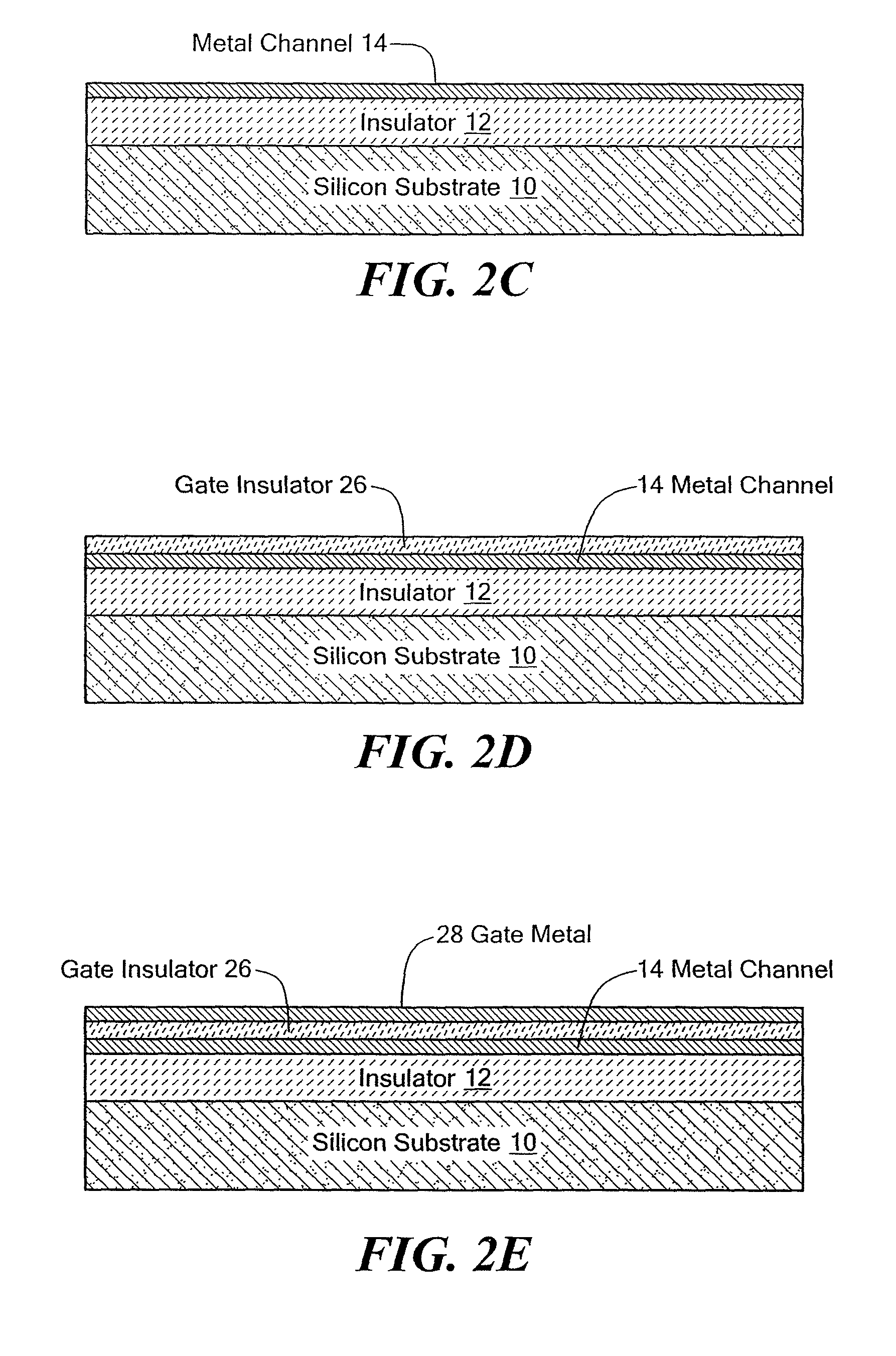
[0008]The present invention related to the use of thin highly
conductive materials that can be selected from the group consisting of metals,
layers of
pure metals, or alloys of
pure metals, doped
pure metals and / or metal silicides, metal salicides, metal nitrides, metal selenides, or metal tellurides (compounds not containing
oxygen) to provide the channel region of a transistor or switching device. The channel region is sufficiently thin that a
reverse bias between a gate and a source
electrode depletes the channel of electrons to switch the transistor “off.” A
voltage between the source and drain with no
gate voltage is applied,
gain is generated. A preferred embodiment of the invention comprises a thin film channel layer having a thickness of less than 5 nm. The metal channel is preferably continuous and can be formed using metals as silver,
copper or
platinum. The metal channel can also comprise a
composite structure such as a plurality of layers of different metals or metal alloys to enable the selection of desired
work function characteristics. The preferred devices operate to control the number of carriers within the channel. By controlling the thickness of the material, preferred embodiments enable the fabrication of depletion and enhancement mode devices.

