Method for cleaning optical element of EUV light source device and optical element cleaning device
a technology of light source device and cleaning method, which is applied in the direction of optical radiation measurement, x-ray tube, spectrophotometry/monochromator, etc. it can solve the problems of difficult to overcome the influence of neutral particles and/or ions emitted from the plasma and target, difficult to maintain, and extremely expensive. , to achieve the effect of prolonging the usable life of the optical element and being easy to overcom
- Summary
- Abstract
- Description
- Claims
- Application Information
AI Technical Summary
Benefits of technology
Problems solved by technology
Method used
Image
Examples
example 1
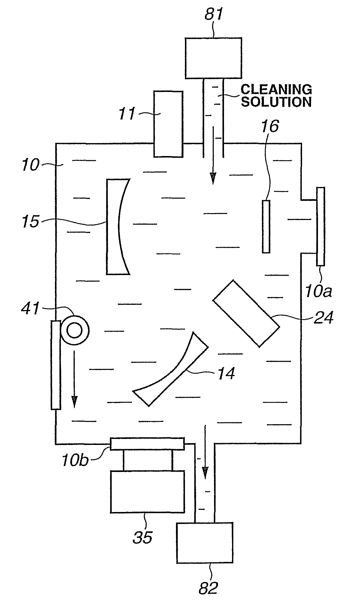
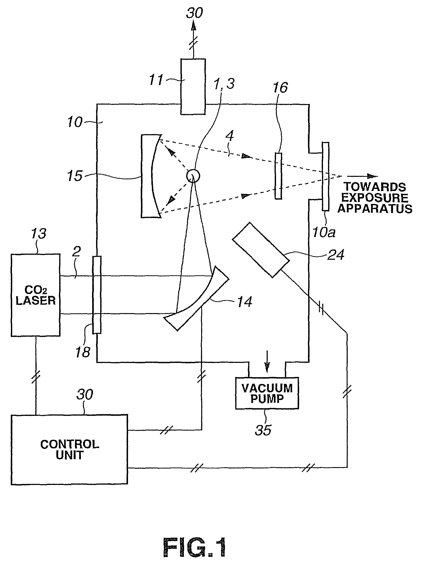
[0066]FIG. 5 is a diagram illustrating the constitution of a first embodiment. In FIG. 5, features identical to those of FIG. 1 are denoted with identical reference numerals, and the explanation thereof is omitted.
[0067]In the present embodiment, the adherence of the nanosize debris adhered to the input window 18 is overcome by wiping the output side surface of the input window 18.
[0068]A scrubber 41 is provided in the vicinity of the input window 18 inside the vacuum chamber 10. The scrubber 41 is a rotary brush comprising a brush 41b of a material such as nylon, mohair, PVA (polyvinyl alcohol), PP (polypropylene) or the like, provided around a cylindrical shaft 41a. A driving device not shown causes the scrubber 41 to slide over the input window 18 while rotating around the shaft axis. The scrubber 41 may be a fixed brush instead of a rotary brush.
[0069]The scrubber 41 may be imparted a weak chemical cleaning effect by wetting the brush 41b with a cleaning solution, for instance, ...
example 2
[0073]FIG. 6 is a diagram illustrating the constitution of a second embodiment. In FIG. 6, features identical to those of FIG. 1 are denoted with identical reference numerals, and the explanation thereof is omitted.
[0074]In the present embodiment, the adherence of nanosize debris to a debris protective plate 46 (having as a material thereof any among ZnSe, BaF2, NaCl, Si, Ge, CsI and KRS-5) provided on the output side of the input window 18 is overcome through wiping of the surface of the debris protective plate 46.
[0075]A cleaning chamber 45 is partitioned off in the interior of the vacuum chamber 10, in the vicinity of the input window 18, in such a way so as not to hinder the laser beam 2. The debris protective plate 46, shaped as a circular plate, is pivotably supported inside the cleaning chamber 45. The debris protective plate 46 is a transmissive optical element formed of, for instance, zinc selenium (ZnSe), barium fluoride or the like (BaF2) or the like. Part of the debris p...
example 3
[0080]FIG. 7 is a diagram illustrating the constitution of a third embodiment. In FIG. 7, features identical to those of FIG. 1 are denoted with identical reference numerals, and the explanation thereof is omitted.
[0081]In the present embodiment, the adherence of nanosize debris adhered to the reflective surface of the EUV collector mirror 15 is overcome by sputtering (plasma etching) in which plasma is biased.
[0082]Inside the vacuum chamber 10 there are provided a planar electrode 51, comprising a conductive substrate, connected to the rear face of the EUV collector mirror 15, and a grid electrode 52 facing the reflective surface of the EUV collector mirror 15, so as to flank the generation region of the plasma 3. The planar electrode 51 is connected to a 13.56 MHz RF power supply 54 via a blocking capacitor 53. The grid electrode 52 is connected to ground. In such a configuration, the planar electrode 51 is the cathode and the grid electrode 52 is the anode.
[0083]A gas supply devi...
PUM
| Property | Measurement | Unit |
|---|---|---|
| wavelength | aaaaa | aaaaa |
| wavelength | aaaaa | aaaaa |
| wavelength | aaaaa | aaaaa |
Abstract
Description
Claims
Application Information
 - R&D
- Intellectual Property
- Life Sciences
- Materials
- Tech Scout
- Unparalleled Data Quality
- Higher Quality Content
- 60% Fewer Hallucinations
Browse by: Latest US Patents, China's latest patents, Technical Efficacy Thesaurus, Application Domain, Technology Topic, Popular Technical Reports.
© 2025 PatSnap. All rights reserved.Legal|Privacy policy|Modern Slavery Act Transparency Statement|Sitemap|About US| Contact US: help@patsnap.com


