Atomic layer deposition of metal oxide materials for memory applications

a metal oxide and memory technology, applied in the field of memory devices, can solve the problems of low resistance metal oxide film not being able to form a reliable nonvolatile memory device, affecting the performance of nonvolatile memory devices, and posing challenges for traditional nonvolatile memory technology, etc., to achieve simple and accurate thickness control, facilitate oxygen vacancy movement or filament formation, and improve switching performance and reliability

Active Publication Date: 2012-10-16
INTERMOLECULAR
View PDF19 Cites 24 Cited by
  • Summary
  • Abstract
  • Description
  • Claims
  • Application Information

AI Technical Summary

Benefits of technology

[0013]The misaligned grain interface disposed between the two metal oxide layers facilitates oxygen vacancy movement or filamentary formation. The misaligned grain interface contains numerous grain boundaries that extend parallel to the electrode interfaces, in contrast to the grains in the bulk film that extend perpendicular to the electrode interfaces. As a result, oxygen vacancies are trapped and released during switching without any overall loss or without significant loss of vacancies. Therefore, the metal oxide film stacks have improved switching performance and reliability during memory cell applications—compared to previous memory cells which generally contain traditional hafnium oxide based stacks.
[0014]The described ALD processes are techniques for depositing ultra-thin metal oxide films due to practical advantages which includes simple and accurate thickness control, precise control of dopant / element concentrations and distributions, excellent reproducibility and uniformity, and capability to produce conformal films at sharp interfaces and trenches with high aspect ratio.
[0017]In one embodiment described herein, a method for fabricating a resistive switching memory element, such as a memory device, is provided and includes forming a metal oxide film stack over a lower electrode disposed on a substrate, wherein the metal oxide film stack contains a metal oxide coupling layer disposed on a metal oxide host layer, and an interface is formed between the metal oxide host layer and the metal oxide coupling layer. The interface facilitates oxygen vacancy between the crystalline metal-rich oxide host material of the metal oxide host layer and the amorphous metal-rich oxide coupling material of the metal oxide coupling layer.
[0025]In another embodiment described herein, a method for fabricating a resistive switching memory element, such as a memory device, is provided and includes forming a metal oxide film stack over a lower electrode disposed on a substrate, wherein the metal oxide film stack contains a metal oxide coupling layer disposed on a metal oxide host layer. A misaligned grain interface is formed between the grain boundary of the metal oxide host layer and the grain boundary of the metal oxide coupling layer. The misaligned grain interface facilitates oxygen vacancy between the metal-rich oxide host material and the metal-rich oxide coupling material. The method further provides forming the metal oxide film stack which includes forming the metal oxide host layer over the lower electrode during a first ALD process, wherein the metal oxide host layer substantially contains a crystalline metal-rich oxide host material having the generic chemical formula of MOx, where M is a metal selected from hafnium, zirconium, or titanium and x may be within a range from about 1.65 to about 1.95.

Problems solved by technology

However, as device dimensions shrink, scaling issues are posing challenges for traditional nonvolatile memory technology.
Although metal oxide films such as these exhibit bistability, the resistance of these films and the ratio of the high-to-low resistance states are often insufficient to be of use within a practical nonvolatile memory device.
Therefore, a low resistance metal oxide film may not form a reliable nonvolatile memory device.
For example, in a nonvolatile memory that has conductive lines formed of a relatively high resistance metal such as tungsten, the resistance of the conductive lines may overwhelm the resistance of the metal oxide resistive switching element.
Therefore, the state of the bistable metal oxide resistive switching element may be difficult or impossible to sense.
Similar issues can arise from integration of the resistive switching memory element with current steering elements, such as diodes and / or resistors.
However, since the power that can be delivered to a circuit containing a series of resistive switching memory elements and current steering elements is typically limited in most conventional nonvolatile memory devices (e.g., CMOS driven devices), it is desirable to form each of the resistive switching memory elements and current steering elements in the circuit so that the voltage drop across each of these elements is small, and thus resistance of the series connected elements does not cause the current to decrease to an undesirable level due to the fixed applied voltage (e.g., about 2-5 volts).
The transition metal oxide materials used within the resistive switching elements have been doped with highly reactive dopant metals which cause problems to the bulk switching layer.
Highly reactive dopant metals may extract oxygen from the bulk switching layer and cause excessive leakage in the resistive switching element.
Also, it is usually difficult to control the removal of appreciable amount of oxygen from the metal oxide films.
If the metal oxide film contains hafnium oxide, the loss of too much oxygen provides an excess hafnium metal which in turn may cause device failure.
The excess hafnium metal may chemical reduces silicon oxide material generally disposed between the bottom electrode and the metal oxide film and turn forms hafnium silicide—which has undesirable properties at this interface.

Method used


Image

  • Atomic layer deposition of metal oxide materials for memory applications
  • Atomic layer deposition of metal oxide materials for memory applications
  • Atomic layer deposition of metal oxide materials for memory applications

Examples


Embodiment Construction

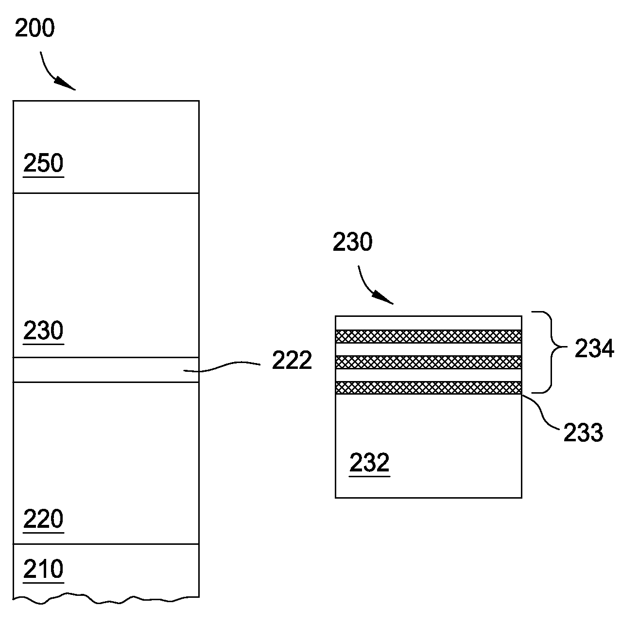
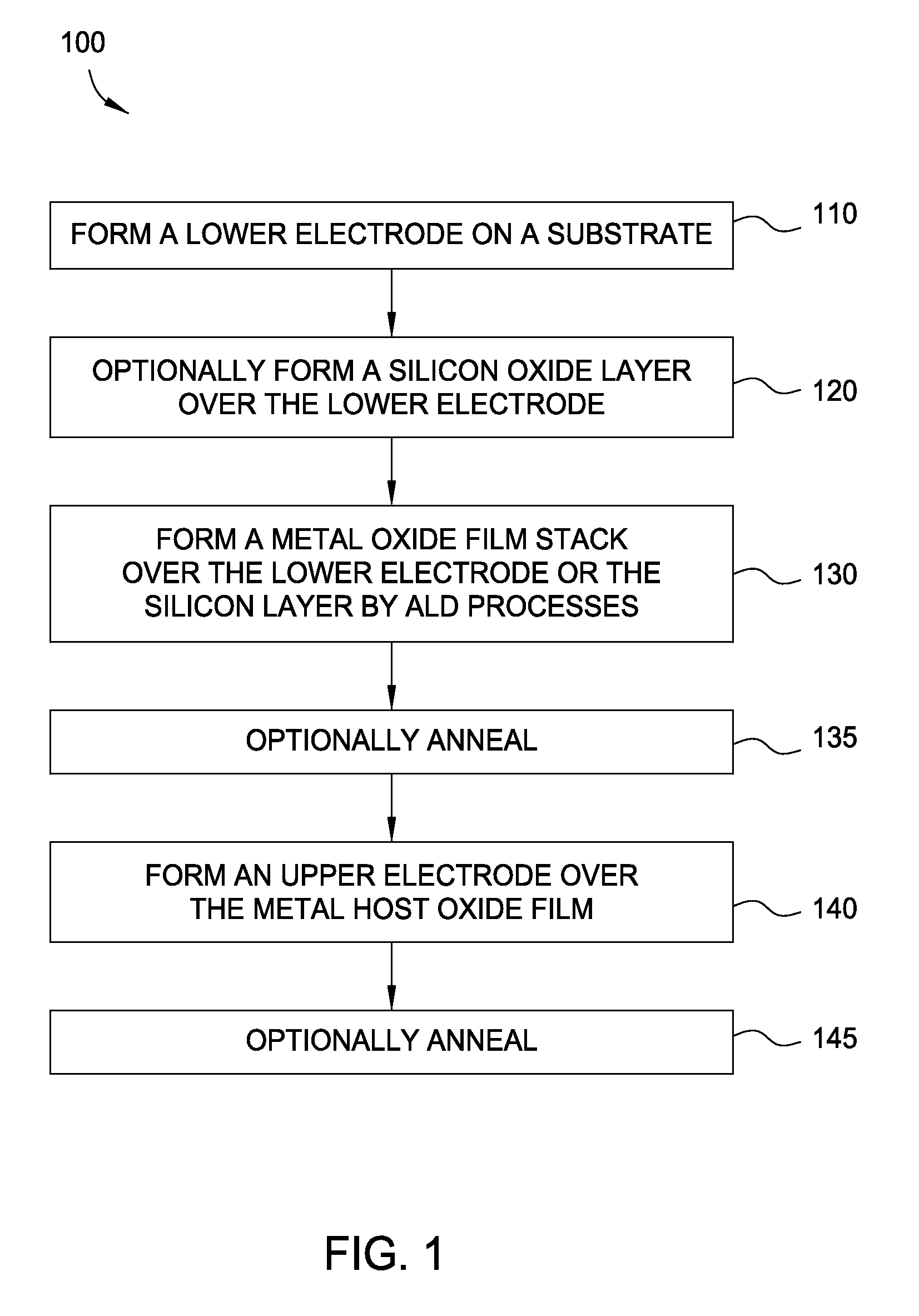
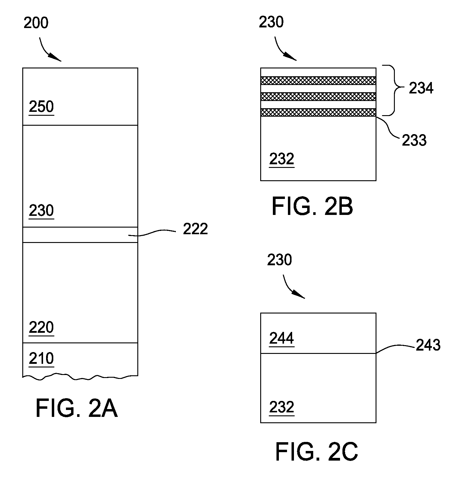
[0036]Embodiments of the invention generally relate to nonvolatile memory devices and methods for manufacturing such memory devices. Embodiments of the invention generally relate to nonvolatile memory devices and methods for manufacturing such memory devices. Embodiments described herein provide methods for forming improved memory devices, such as a ReRAM cells, and also provide optimized, atomic layer deposition (ALD) processes for forming metal oxide film stacks. The metal oxide film stacks described herein contain at least two metal oxide layers adjacent to or in contact with each other, such as a metal oxide coupling layer disposed on a metal oxide host layer. The metal oxide layers contain different metal oxide materials and each metal oxide material has a different grain structure and / or size from the other—therefore the metal oxide layers have a grain boundary disposed at the interface therebetween.

[0037]The interface disposed between the two metal oxide layers facilitates ox...


PUM

PropertyMeasurementUnit
grain sizeaaaaaaaaaa
temperatureaaaaaaaaaa

Abstract

Embodiments of the invention generally relate to nonvolatile memory devices, such as a ReRAM cells, and methods for manufacturing such memory devices, which includes optimized, atomic layer deposition (ALD) processes for forming metal oxide film stacks. The metal oxide film stacks contain a metal oxide coupling layer disposed on a metal oxide host layer, each layer having different grain structures / sizes. The interface disposed between the metal oxide layers facilitates oxygen vacancy movement. In many examples, the interface is a misaligned grain interface containing numerous grain boundaries extending parallel to the electrode interfaces, in contrast to the grains in the bulk film extending perpendicular to the electrode interfaces. As a result, oxygen vacancies are trapped and released during switching without significant loss of vacancies. Therefore, the metal oxide film stacks have improved switching performance and reliability during memory cell applications compared to traditional hafnium oxide based stacks of previous memory cells.

Description

BACKGROUND OF THE INVENTION[0001]1. Field of the Invention[0002]Embodiments of the invention generally relate to memory devices and methods for manufacturing such memory devices.[0003]2. Description of the Related Art[0004]Nonvolatile memory elements are used in systems in which persistent storage is required. For example, digital cameras use nonvolatile memory cards to store images and digital music players use nonvolatile memory to store audio data. Nonvolatile memory is also used to persistently store data in computer environments. Nonvolatile memory is often formed using electrically-erasable programmable read only memory (EPROM) technology. This type of nonvolatile memory contains floating gate transistors that can be selectively programmed or erased by application of suitable voltages to their terminals.[0005]As fabrication techniques improve, it is becoming possible to fabricate nonvolatile memory elements with increasingly smaller dimensions. However, as device dimensions sh...

Claims


Application Information

Patent Timeline
Patent Type & Authority Patents(United States)
IPC IPC(8): H01L21/31H01L21/469
CPCC23C16/40H01L45/145H01L21/02178H01L21/02181H01L21/02186H01L21/02189H01L21/02192H01L21/02194H01L21/022H01L21/0228H01L45/08H01L45/1266H01L45/146H01L45/1616H01L45/1608H01L21/02175C23C16/45525H01L27/2463H10B63/80H10N70/24H10N70/8416H10N70/8833H10N70/023H01L21/28556H10N70/883H10N70/021
Inventor WANG, YUNGOPAL, VIDYUTHASHIM, IMRANPRAMANIK, DIPANKARCHIAG, TONY
Owner INTERMOLECULAR
Why Eureka
Try Eureka