Semiconductor device

a technology of semiconductors and devices, applied in pulse manipulation, power consumption reduction, pulse technique, etc., can solve problems such as power consumption increase, and achieve the effect of low power consumption

Active Publication Date: 2015-03-24
SEMICON ENERGY LAB CO LTD
View PDF129 Cites 23 Cited by
  • Summary
  • Abstract
  • Description
  • Claims
  • Application Information

AI Technical Summary

Benefits of technology

[0010]In the inverter circuit in which all the transistors have the same conductivity type, the driving frequency is lowered because the rise time of an output signal of the inverter circuit becomes longer when one of the transistors is turned on. Moreover, power consumption is increased because of the off-state leakage current of one or the other of the transistors.
[0032]According to one embodiment of the present invention, it is possible to provide a semiconductor device including a logic circuit whose driving frequency is increased by control of the threshold voltage of a transistor. In addition, it is possible to provide a semiconductor device including a logic circuit with low power consumption.

Problems solved by technology

Moreover, power consumption is increased because of the off-state leakage current of one or the other of the transistors.

Method used


Image

  • Semiconductor device
  • Semiconductor device
  • Semiconductor device

Examples


embodiment 1

(Embodiment 1)

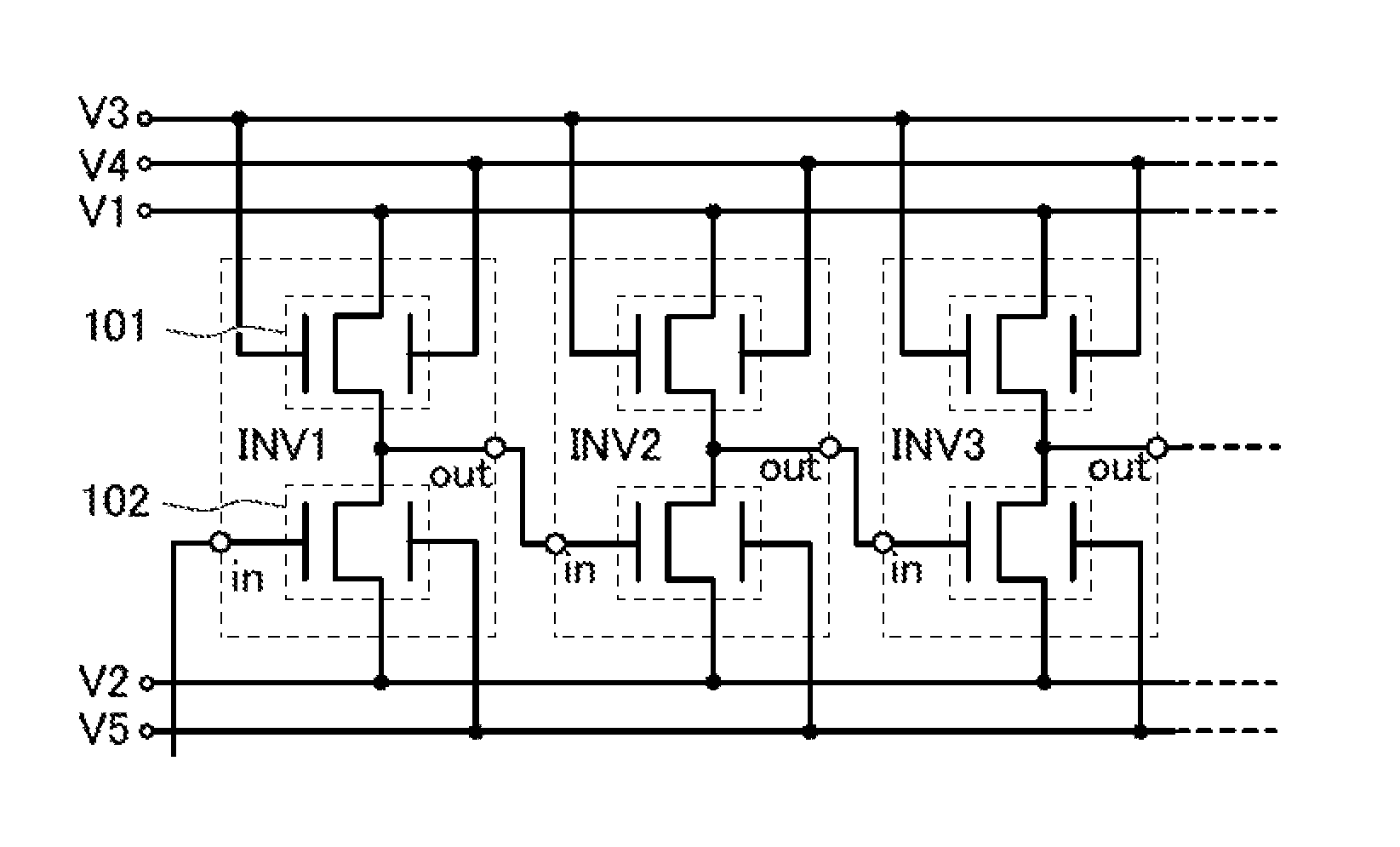
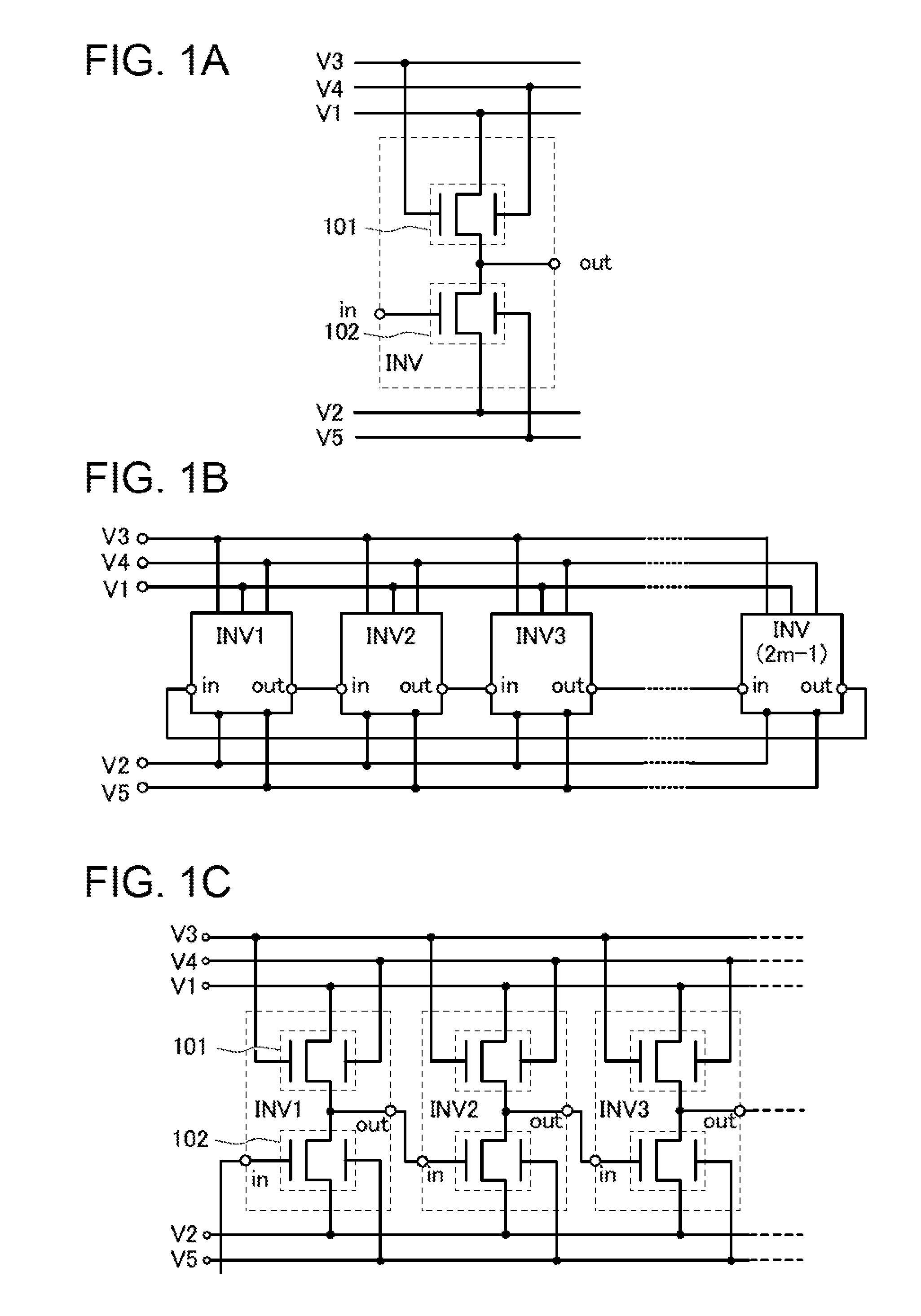
[0060]In this embodiment, a ring oscillator according to one embodiment of the present invention will be described with reference to FIGS. 1A to 1C and FIGS. 2A to 2C. A ring oscillator illustrated in FIGS. 1B and 1C includes an inverter circuit INV illustrated in FIG. 1A as an inverter circuit; therefore, the inverter circuit INV illustrated in FIG. 1A will be described first.

[0061]FIG. 1A is a circuit diagram illustrating a specific configuration of the inverter circuit INV. The inverter circuit INV includes a transistor 101 and a transistor 102. In the inverter circuit INV, the transistor 101 and the transistor 102 are connected in series between a power supply line V1 supplied with a power supply potential V1 and a power supply line V2 supplied with a power supply potential V2. In other words, a source electrode of the transistor 101 and a drain electrode of the transistor 102 are electrically connected to each other.

[0062]The transistor 101 and the transistor 102 ...

embodiment 2

(Embodiment 2)

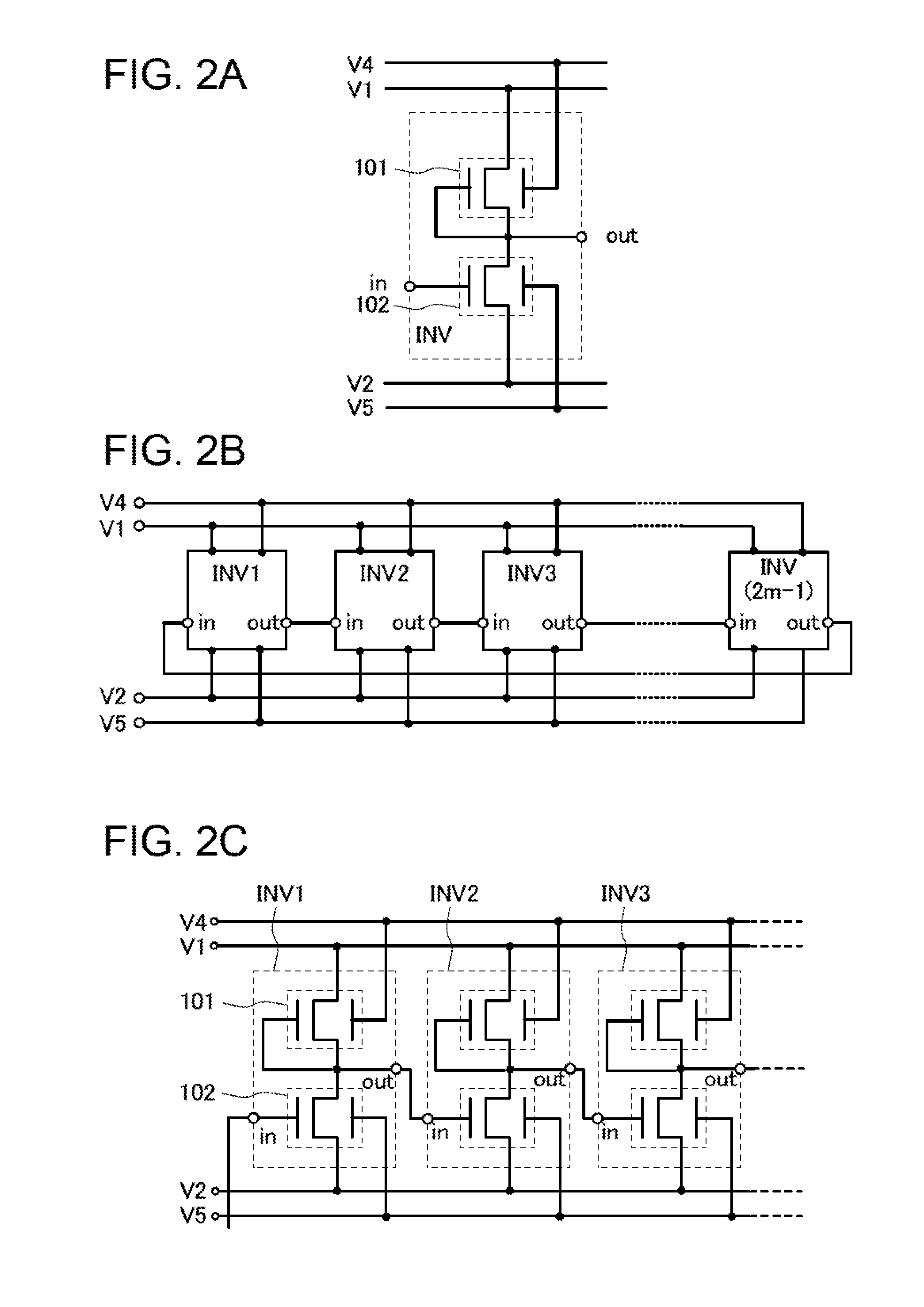
[0093]In this embodiment, ring oscillators different from those in Embodiment 1 will be described with reference to FIGS. 3A and 3B, FIG. 4, FIGS. 5A and 5B, and FIGS. 6A and 6B.

[0094]A ring oscillator illustrated in FIG. 3B includes an inverter circuit INVa and a control inverter circuit INVb illustrated in FIG. 3A; the control inverter circuit INVb is used to control a voltage applied to the second gate electrode of the transistor 101 included in the inverter circuit INVa. First, the inverter circuit INVa and the control inverter circuit INVb illustrated in FIG. 3A will be described.

[0095]FIG. 3A is a circuit diagram illustrating specific configurations of the inverter circuit INVa and the control inverter circuit INVb. The inverter circuit INVa includes the transistor 101 and the transistor 102. The control inverter circuit INVb includes a transistor 103 and a transistor 104. In the inverter circuit INVa, the transistor 101 and the transistor 102 are connected in se...

embodiment (

3)

[0155]In this embodiment, a method for fabricating a transistor used in the ring oscillator shown in Embodiments 1 and 2 will be described.

[0156]First, an insulating film 401 is formed over a substrate 400 (see FIG. 7A).

[0157]Examples of the substrate 400 are a single crystal semiconductor substrate and a polycrystalline semiconductor substrate containing silicon, silicon carbide, or the like; and a compound semiconductor substrate containing silicon germanium, gallium arsenide, indium phosphide, or the like. Other examples of the substrate 400 are a variety of glass substrates used in the electronics industry, such as substrates of aluminosilicate glass, aluminoborosilicate glass, and barium borosilicate glass, a quartz substrate, a ceramic substrate, and a sapphire substrate.

[0158]The insulating film 401 is formed with a single-layer structure or a stacked structure using silicon oxide, silicon oxynitride, silicon nitride, and / or the like. The insulating film 401 is formed by th...


PUM


Abstract

To provide a semiconductor device including an inverter circuit whose driving frequency is increased by control of the threshold voltage of a transistor or a semiconductor device including an inveter circuit with low power consumption. An inverter circuit includes a first transistor and a second transistor each including a semiconductor film in which a channel is formed, a pair of gate electrodes between which the semiconductor film is placed, and source and drain electrodes in contact with the semiconductor film. Controlling potentials applied to the pair of gate electrodes makes the first transistor have normally-on characteristics and the second transistor have normally-off characteristics. Thus, the driving frequency of the inverter circuit is increased.

Description

BACKGROUND OF THE INVENTION[0001]1. Field of the Invention[0002]The present invention relates to a semiconductor device including a logic circuit.[0003]2. Description of the Related Art[0004]Techniques for fabricating transistors with the use of a semiconductor thin film formed over a substrate having an insulating surface have advanced in recent years, and such transistors are widely used in electronic devices such as integrated circuits (ICs) and image display devices (display devices).[0005]As a semiconductor material that can be applied to transistors, silicon is widely known. As other materials, oxide semiconductors such as indium oxide and zinc oxide and III-V compound semiconductors such as gallium arsenide have attracted attention.[0006]For example, Patent Document 1 discloses a transistor using an amorphous oxide semiconductor containing indium (In), gallium (Ga), and zinc (Zn).[0007]Note that transistors formed using the above oxide semiconductor are n-channel transistors....

Claims


Application Information

Patent Timeline
Patent Type & Authority Patents(United States)
IPC IPC(8): H03K3/03H01L27/088H01L27/12H01L29/786
CPCH01L29/786H01L27/088H01L27/1225H03K19/0013H03K19/20H03K2217/0018H03K2005/00032H03K2005/00195H01L27/124H01L29/7869H03K3/0315
Inventor OHMARU, TAKURONAGATSUKA, SHUHEI
Owner SEMICON ENERGY LAB CO LTD
Why Eureka
Try Eureka