Oxide heat insulation layer for reducing phase-change memory cell power consumption and implementation method thereof

A technology of phase change memory and implementation method, which is applied in the field of microelectronics nanomaterials and device preparation, and can solve problems such as poor effect

Inactive Publication Date: 2008-07-23
SHANGHAI INST OF MICROSYSTEM & INFORMATION TECH CHINESE ACAD OF SCI
View PDF0 Cites 18 Cited by
  • Summary
  • Abstract
  • Description
  • Claims
  • Application Information

AI Technical Summary

Problems solved by technology

But the effect is not good, the present invention tries to achieve better thermal effe...

Method used


Image

  • Oxide heat insulation layer for reducing phase-change memory cell power consumption and implementation method thereof
  • Oxide heat insulation layer for reducing phase-change memory cell power consumption and implementation method thereof
  • Oxide heat insulation layer for reducing phase-change memory cell power consumption and implementation method thereof

Examples


Embodiment 1

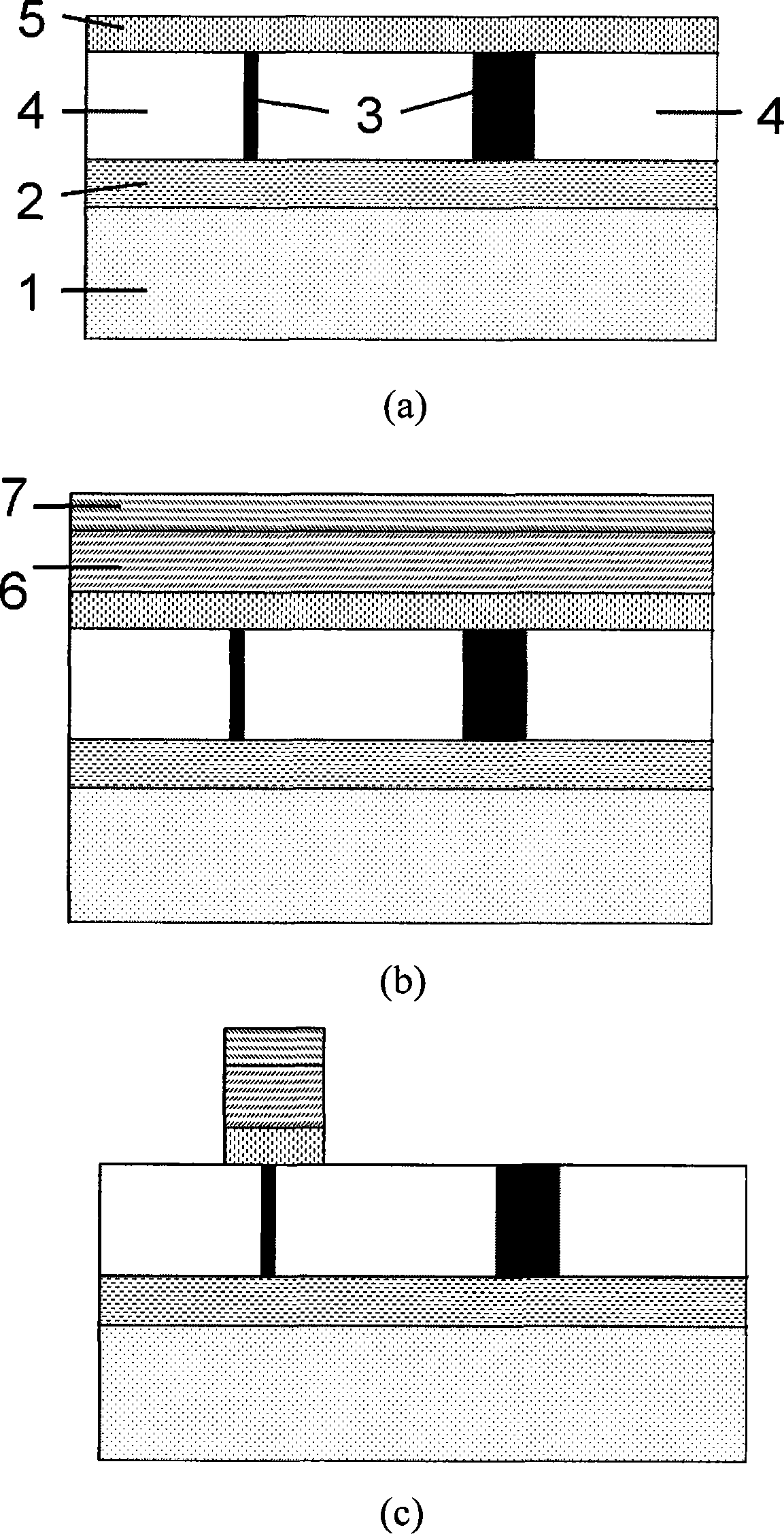
[0032] (1) Use acetone and alcohol solution to clean the substrate for 3 minutes each under the action of ultrasonic waves, then bake at 120°C for 20 minutes, and then deposit the heat-shielding layer oxide material on the substrate by magnetron sputtering Metal element material with a thickness of 4-5nm and a background vacuum of 4×10 during sputtering -6 Torr, the vacuum is 0.18Pa during sputtering, and then oxidized at 580°C for 10 minutes in a high-purity oxygen (>99.995%) atmosphere. Insulation layer material is TiO 2 Wait;

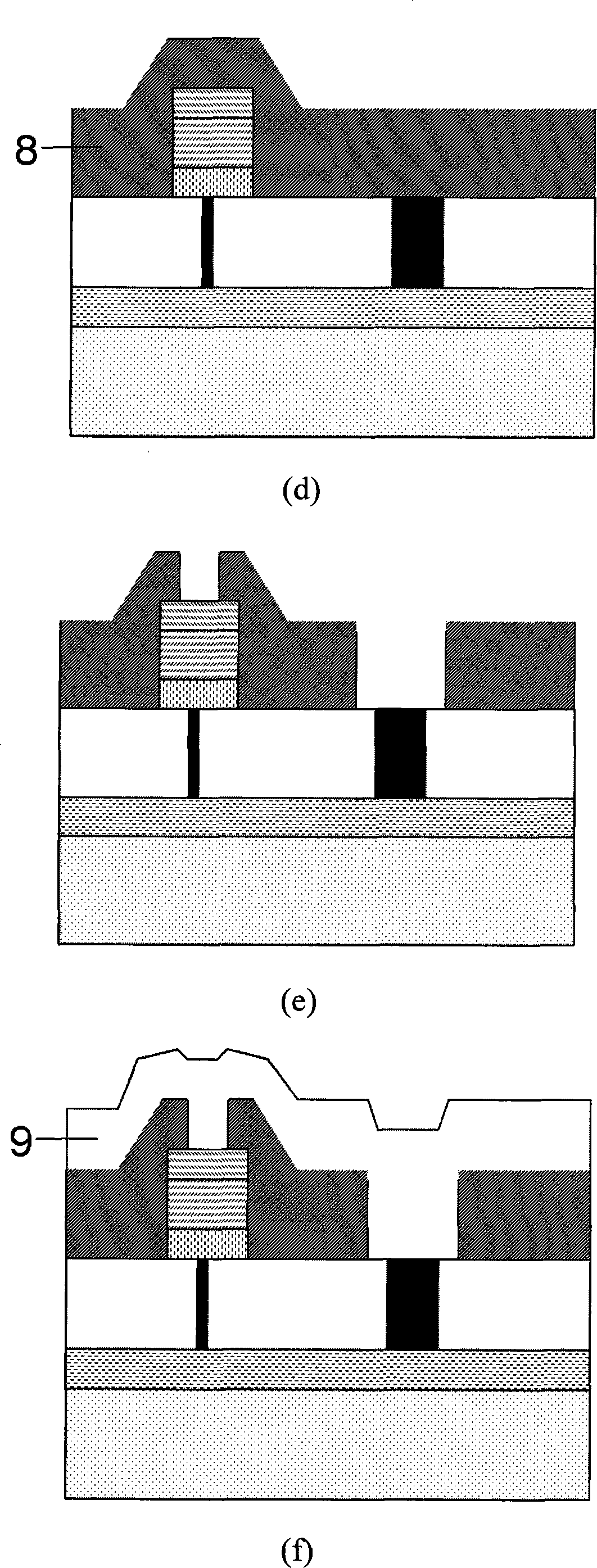
[0033] (2) Use magnetron sputtering method to deposit chalcogenide compound thin film layer 200nm and TiN thin film layer 20nm successively on the oxide insulation layer; the background vacuum is 4×10 during sputtering -6 Torr, the vacuum during sputtering is 0.16Pa and 0.40Pa, and the sputtering power is 200W and 400W respectively; (Figure 1, b)

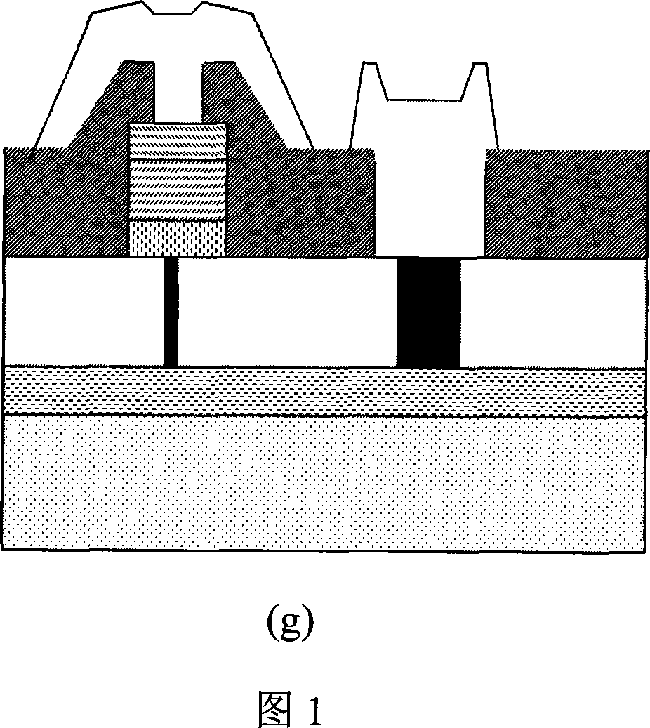
[0034] (3) Use ultraviolet exposure photolithography to etch a square with a side length of 3-5 μm, ...


PUM

PropertyMeasurementUnit
Thicknessaaaaaaaaaa
Thicknessaaaaaaaaaa

Abstract

The invention relates to an oxide insulating layer which is capable of being used to discover a material which reduces the power of a phase change memory and an improvement on the structure of an unit device and an implementation method, and belongs to the field of microelectronics. The invention is characterized in that the oxide insulating layer is added between a bottom heating W electrode and a chalcogenide compound thin film layer, and the thickness of the insulating layer is controlled below 10nm. The optional materials of the oxide insulating layer comprise TiO2 and the like. The improvement of the unit device is achieved through that after various needed thin films are deposited on a substrate, a phase change operation unit in micron is obtained through a micro-nano processing technology, and an upper electrode and a lower electrode which are capable of being used to test the performance are led. Because the oxide insulating layer has excellent thermal stability and thermal conduction which is far lower than a bottom heating W electrode, is compatible with a CMOS standard manufacturing technology, increases marked effect of the unit thermal effect of the device, and the purpose of effectively reducing the power of the unit is achieved.

Description

technical field [0001] The invention relates to an oxide heat-insulating layer for reducing power consumption of a phase-change memory unit and a method for realizing it, and belongs to the field of microelectronics nanometer materials and device preparation. Background technique [0002] Phase Change Memory (PCM) technology is based on S.R.Ovshinsky in the late 1960s (Phys.Rev.Lett.21, 1450-1453, 1968) and early 1970s (Appl.Phys.Lett.18, 254- 257, 1971) proposed that phase-change thin films can be applied to phase-change storage media. Compared with the current dynamic random access memory (DRAM) and flash memory (FLASH), phase change memory has obvious advantages: small size, low driving voltage, low power consumption, fast read and write speed, and non-volatile characteristics. PCM is not only a non-volatile memory, it can resist high and low temperature shock, radiation and vibration, so it will not only be widely used in civilian daily portable electronic products, but...

Claims


Application Information

Patent Timeline
IPC IPC(8): H01L45/00H01L27/24H01L21/82G11C11/56G11C16/02
Inventor 宋志棠徐成刘波封松林
Owner SHANGHAI INST OF MICROSYSTEM & INFORMATION TECH CHINESE ACAD OF SCI
Why Eureka
Try Eureka