Growth of SiO2 nanometer mask in gallium nitride film by HVPE method and method thereof

A gallium nitride and mask technology, which is applied in the field of SiO2 nanoparticle lattice mask and preparation, can solve the problems that it is difficult to prepare and obtain a nanoscale mask structure, affect the quality of lateral overgrowth, and complicate the process, and achieve The electrochemical corrosion process is simple, the availability is improved, and the effect of uniform distribution

Inactive Publication Date: 2008-12-10
DAHOM FUJIAN ILLUMINATION TECH
View PDF0 Cites 15 Cited by
  • Summary
  • Abstract
  • Description
  • Claims
  • Application Information

AI Technical Summary

Problems solved by technology

In addition, there are many methods to reduce the dislocation density, but they are all similar to the lateral epitaxy overgrowth (ELOG) technology, but most of them require photolithography and other processes, the process is complicated and the cost is high, and the traditional photolithography method is difficult to prepare nanometer scale mask structure
On the othe...

Method used


Image

  • Growth of SiO2 nanometer mask in gallium nitride film by HVPE method and method thereof

Examples


Embodiment 1

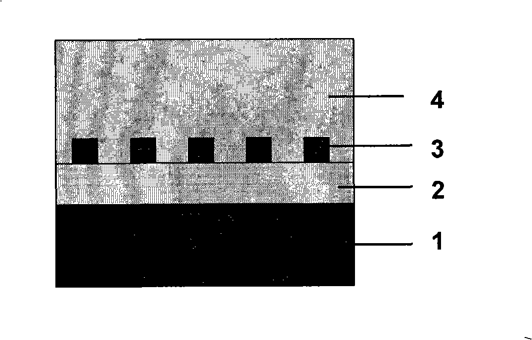
[0018] Using MOCVD method HVPE method or MBE method in Al 2 o 3 A GaN film of about 3 microns was grown on the substrate (0001), and this film was used as a HVPE template, and then a 300nm-thick metal Al thin layer was deposited on this template by electron beam evaporation at a temperature of 200°C, and then the Put the template with Al layer into oxalic acid solution (0.3mol / L) or sulfuric acid solution (15wt%), and use a voltage of 40 volts to carry out anodic oxidation for about 15 minutes at room temperature, then the metal Al is electrochemically corroded into regularly distributed porous AAO, and then soak the template in phosphoric acid solution (5wt%) at 30°C for 40min, the purpose is to expand the pore size and remove the part of the aluminum oxide at the bottom of the small hole that is in contact with the lower layer of GaN. After cleaning, deposit 3- 10nm thick SiO 2 , and finally soaked in 20% hydrochloric acid solution for 60min to remove the AAO layer to form...

Embodiment 2

[0020] Use SiC, Si or GaAs as the substrate, and the rest are the same as in Embodiment 1.


PUM

PropertyMeasurementUnit
Thicknessaaaaaaaaaa
Thicknessaaaaaaaaaa

Abstract

The invention relates to a silicon dioxide nano particle dot matrix mask used in a GaN film of hydride gas phase epitaxial growth, and a preparation method thereof, characterized by that a SiO2 nano particle lattie is used as a mask for GaN transversely epitaxial over growth. A layer of metal Al is evaporated by electron beam on a GaN form board firstly. Porous anode alumina (AAO) is prepared by electrochemistry then. A layer of dielectric SiO2 layer is deposited then. AAO is removed by acid solutionor aqueous alkali. Therefore, dot matrix distribution of SiO2 nano particle is obtained on the GaN form board. After cleaning treatment, the form board as a substrate is put in a HVPE reaction chamber for GaN thick film growth. The invention simplifies the photo-etching mask manufacturing technology greatly, and reduces the size of the mask to nanometer level, while metal Al and SiO2 layer can be prepared through electron beam evaporation and sputtering method for batched production.

Description

technical field [0001] The invention relates to a hydride vapor phase epitaxy (HVPE) method for growing SiO in gallium nitride (GaN) films 2 Nanoparticle lattice mask and its preparation method. The invention aims at improving the quality of epitaxially grown GaN materials, and belongs to the field of GaN film preparation. Background technique [0002] GaN material has excellent characteristics such as high luminous efficiency, high thermal conductivity, high temperature resistance, radiation resistance, acid and alkali resistance, high strength and high hardness. In recent years, it has attracted attention as the most advanced semiconductor material in the world. , green, purple, white light-emitting diodes and lasers, GaN has received more applications and attention. However, currently GaN still relies on Al 2 o 3 , GaAs, SiC, Si and other heterogeneous substrates, due to their large lattice mismatch and thermal expansion mismatch coefficients with GaN materials, in th...

Claims


Application Information

Patent Timeline
IPC IPC(8): H01L21/205
Inventor 王新中于广辉林朝通曹明霞巩航齐鸣李爱珍
Owner DAHOM FUJIAN ILLUMINATION TECH
Why Eureka
Try Eureka