

Photo-curing ink-jet nano conductive printing ink, and preparation and use method thereof
A nano-conductive and light-curing technology, applied in ink, printed circuit manufacturing, application, etc., can solve the problems of high temperature resistance of substrate materials, slow curing speed of thermosetting resin, high curing temperature of thermosetting resin, etc., to achieve shortening Effects of sintering time, lower sintering temperature, and higher resolution
- Summary
- Abstract
- Description
- Claims
- Application Information
AI Technical Summary
Problems solved by technology
Method used
Image

Examples
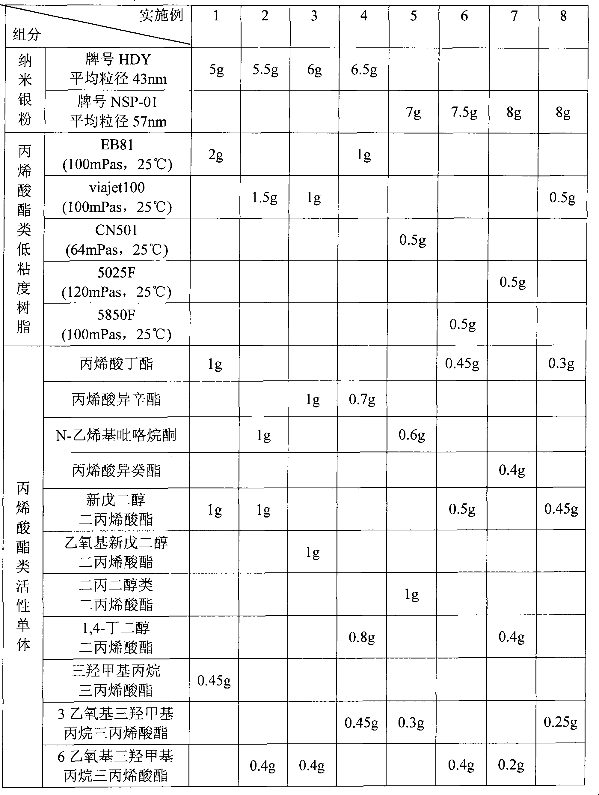
Embodiment 1
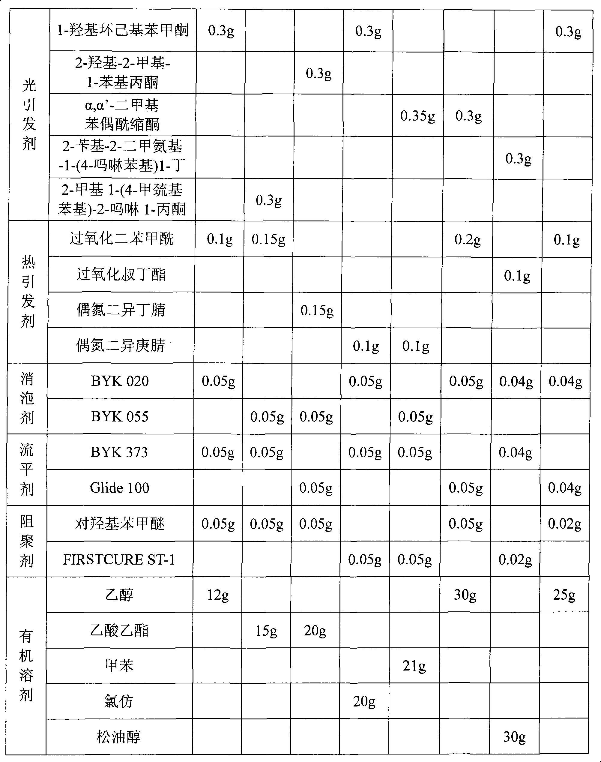
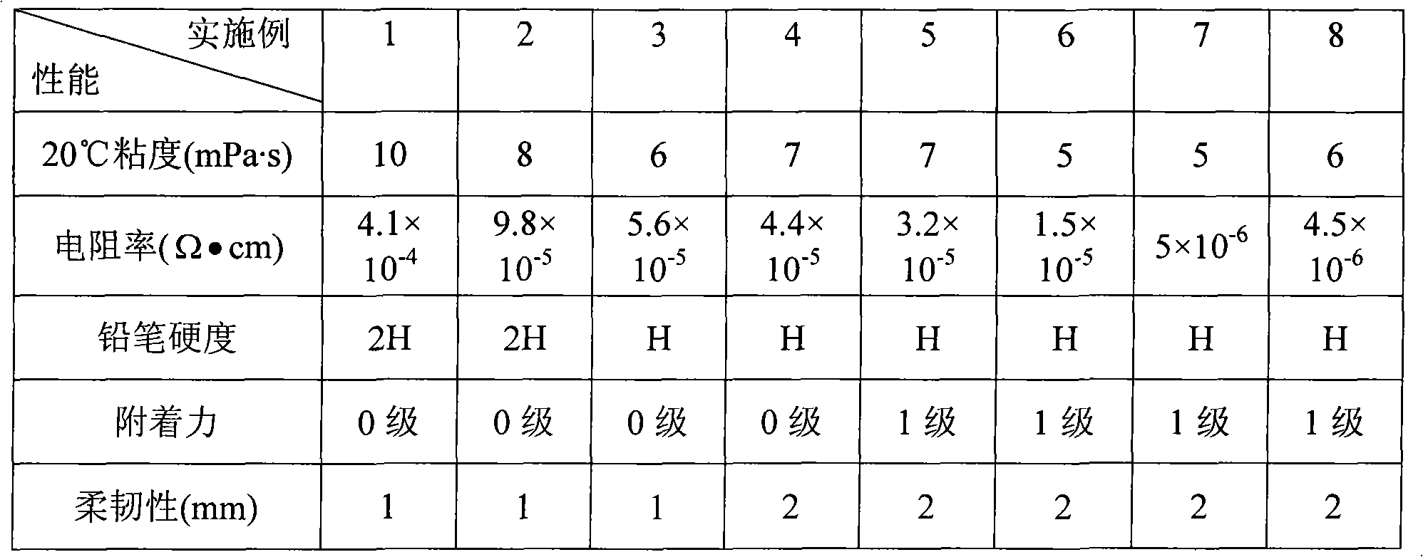
[0042] Firstly, 5g of nano-silver powder (brand HDY, average particle size 43nm) was dissolved in 12g of ethanol and ultrasonically dispersed for 20 minutes to a homogeneous solution, and then added acrylic low-viscosity resin EB81 under the condition of yellow light (filtering light with a wavelength less than 420nm) (100mPas, 25°C) 2g, butyl acrylate 1g, neopentyl glycol diacrylate 1g, trimethylolpropane triacrylate 0.45g, 1-hydroxycyclohexyl benzophenone 0.3g, dibenzoyl peroxide 0.1g, BYK 020 0.05g, BYK 373 0.05g, and p-hydroxyanisole 0.05g were stirred evenly, and then ultrasonically dispersed for 15 minutes to prepare a photocurable inkjet nano conductive ink with a viscosity (20°C) of 10mPa·s.
[0043] Spray the prepared photocurable inkjet nano-conductive ink on the surface of the glass substrate with an inkjet printer, expose it to a high-pressure mercury lamp (the main wavelength is 365nm) for 2 minutes, and then sinter it on a temperature-controllable heating table at...
Embodiment 2
[0045] First, 5.5g of nano-silver powder (brand HDY, average particle size 43nm) was dissolved in 15g of ethyl acetate and ultrasonically dispersed for 20 minutes to a homogeneous solution. Viscosity resin viajet100 (100mPas, 25°C) 1.5g, N-vinylpyrrolidone 1g, neopentyl glycol diacrylate 1g, 6-ethoxytrimethylolpropane triacrylate 0.4g, 2-methyl 1-( 0.3g of 4-methylmercaptophenyl)-2-morpholine 1-acetone, 0.15g of dibenzoyl peroxide, 0.05g of BYK 055, 0.05g of BYK 373, 0.05g of p-hydroxyanisole, stir well and then ultrasonically disperse After 20 minutes, a photocurable inkjet nano conductive ink was prepared, with a viscosity (20° C.) of 8 mPa·s.
[0046] Spray the prepared photocurable inkjet nano-conductive ink on the surface of the glass substrate with an inkjet printer, expose it to a high-pressure mercury lamp (the main wavelength is 365nm) for 2 minutes, and then sinter it on a temperature-controllable heating table at 180°C. 10min to get the experimental sample. Resist...
Embodiment 3
[0048] First, 6g of nano-silver powder (brand HDY, average particle size 43nm) was dissolved in 20g of ethyl acetate and ultrasonically dispersed for 20 minutes to a homogeneous solution, and then added acrylate low-viscosity Resin viajet100 (100mPas, 25°C) 1g, isooctyl acrylate 1g, ethoxy neopentyl glycol diacrylate 1g, 6-ethoxytrimethylolpropane triacrylate 0.4g, 2-hydroxy-2-methyl 0.3g of 1-phenylacetone, 0.15g of azobisisobutyronitrile, 0.05g of BYK 055, 0.05g of Glide 100, 0.05g of p-hydroxyanisole were stirred evenly, and then ultrasonically dispersed for 20 minutes to obtain a photocurable spray Ink nano conductive ink, the viscosity (20°C) is 6mPa·s.
[0049] Spray the prepared photocurable inkjet nano-conductive ink on the surface of the polyester film with an inkjet printer, expose it to a high-pressure mercury lamp (the main wavelength is 365nm) for 100s, and then place it on a temperature-controllable heating table at 150°C. Sinter for 10 minutes to obtain an expe...
PUM
| Property | Measurement | Unit |
|---|---|---|
| Viscosity | aaaaa | aaaaa |
| Resistivity | aaaaa | aaaaa |
| Flexibility | aaaaa | aaaaa |
Abstract
Description
Claims
Application Information