
Improved carbon nanotube based semiconducting devices and methods for their production

A technology of carbon nanotubes and nanotubes, which is applied in the field of improved photovoltaic devices or light-emitting devices, can solve the problems of prolonged exposure, deterioration of absorption and/or emission characteristics, etc., and achieve the goals of prolonging device life, good operational stability, and improving performance Effect

Inactive Publication Date: 2012-04-25
UNIVERSITY OF SURREY
View PDF6 Cites 0 Cited by
  • Summary
  • Abstract
  • Description
  • Claims
  • Application Information

AI Technical Summary

Problems solved by technology

That is, prolonged exposure leads to degradation of the chromophoric moieties in the organic material, leading to an irreversible deterioration of its absorption and / or emission properties

Method used


Image

  • Improved carbon nanotube based semiconducting devices and methods for their production
  • Improved carbon nanotube based semiconducting devices and methods for their production
  • Improved carbon nanotube based semiconducting devices and methods for their production

Examples


no. 1 approach

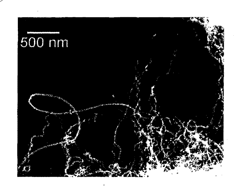
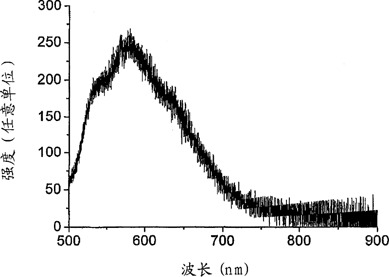
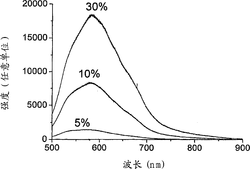
[0059] In this embodiment, tuned carbon nanotubes embedded in an organic matrix are excited into electronically excited states by coherent visible and ultraviolet light. It should be noted, however, that in the present invention, photoexcitation of tuned carbon nanotubes can be achieved using coherent light (such as laser light) and / or incoherent light (such as sunlight). The photoexcited carbon nanotubes then transfer the excitation energy, at least a portion of it, to emissive centers in the organic matrix, which then return to the ground state upon emission of visible light. In this embodiment, the energy of light emitted by the organic host matrix is ​​lower than the energy absorbed by the tuned carbon nanotubes. That is, in this embodiment, the tuned composite of carbon nanotubes and organic matrix is ​​used as a downconverter for UV and visible light.

[0060] To fabricate composites in which carbon nanotubes are dispersed in a matrix of organic materials requires sever...

no. 2 approach

[0077] Utilize the present invention to make organic solar cells:

[0078] Organic solar cells include one or more semiconducting organic thin films sandwiched between two electrodes. Each film may comprise a single material or a composite of two or more different materials.

[0079] Figure 12A A schematic diagram of a heterojunction organic solar cell device according to the present embodiment is shown. The device includes a transparent anode 301 made of indium tin oxide (ITO) coated glass with a sheet resistance of less than 100 ohms / square. The ITO coating on the glass substrate is usually 100nm-300nm thick. It should be understood that any translucent conductive substrate can be used as a transparent electrode, including conductive polymer-carbon nanotube composites such as poly(3,4-ethylenedioxy-2,4-thiophene)-polyphenylene Ethylene sulfonate (PEDOT:PSS)-MWCNT composites in which a continuous network of MWCNTs in a conductive polymer film is used to enhance its elect...

no. 3 approach

[0087] As described in this embodiment mode, the present invention can also be used in organic light emitting diodes (OLEDs).

[0088] Organic light emitting diodes include one or more semiconducting organic films sandwiched between two electrodes. Each membrane may contain a single compound or a composite of two or more different compounds.

[0089] Figure 13A A schematic diagram of a multilayer OLED device according to the present embodiment is shown. The device includes a transparent anode 901 made of indium tin oxide (ITO) coated glass with a sheet resistance of less than 100 ohms / square. The ITO coating on the glass substrate is usually 100nm-300nm thick. Next to the transparent anode 901 are two organic layers: a hole transport layer 902 and an emitter layer 903 . In this embodiment, the emitter layer comprises a composite of tuned carbon nanotubes and an organic semiconductor. The device is completed by a low work function metal cathode 904 . An external power so...


PUM

PropertyMeasurementUnit
thicknessaaaaaaaaaa

Abstract

A method of producing a photo-voltaic device comprising the steps of: synthesising carbon nanotubes; adapting the synthesised carbon nanotubes to provide a surface defect such as to create an effective band gap; selecting an organic semiconductor material which facilitates the efficient energy transfer between carbon nanotubes and the organic material, wherein the organic material is selected such that the energy band gap formed between the HOMO and LUMO energy levels lies within the effective band gap of the adapted carbon nanotubes; combining the adapted carbon nanotubes and the selected organic material to form a composite material.

Description

technical field [0001] The present invention relates to improved photovoltaic or light emitting devices and methods of their manufacture. In particular, the present invention relates to methods in which carbon nanotubes are combined with selected semiconducting organic materials to form composite materials. Background technique [0002] It should be noted that in this application, carbon nanotubes (CNTs) mean single-walled conductive or semiconductive carbon nanotubes (SWCNTs), multi-walled carbon nanotubes (MWCNTs) or a mixture of both. It should also be noted that the present invention is not limited to CNTs of any particular length or diameter. Furthermore, since carbon nanotubes can be synthesized by several different methods, such as chemical vapor deposition (CVD), arc discharge, and laser ablation, it should be noted that the present application is not limited to any particular method of making carbon nanotubes. [0003] It should also be noted that in this applicat...

Claims


Application Information

Patent Timeline
Patent Type & Authority Patents(China)
IPC IPC(8): H01L51/00H01L51/42H01L51/50
CPCB82Y10/00H01L51/5036H01L51/447H01L51/0037H01L51/0047H01L51/4246H01L51/4253H01L51/0049Y02E10/549Y02P70/50H10K85/225H10K85/1135H10K85/215H10K30/211H10K30/87H10K30/30H10K50/125H10K85/221H10K50/00H10K85/20
Inventor 罗斯·安德鲁·哈顿森布提拉切莱格·拉维·希尔瓦西蒙·约翰·亨里
Owner UNIVERSITY OF SURREY
Learn More