Method for preparing high depth-to-width ratio carbon micro electro-mechanical device

A high aspect ratio, electrical device technology, applied in the direction of microlithography exposure equipment, photolithography coating equipment, microstructure technology, etc., can solve high cost, substrate desorption, high aspect ratio MEMS device process complexity and other issues, to achieve the effect of low cost, fine graphics, and improved service life

Inactive Publication Date: 2009-07-08
HUAZHONG UNIV OF SCI & TECH
View PDF1 Cites 25 Cited by
  • Summary
  • Abstract
  • Description
  • Claims
  • Application Information

AI Technical Summary

Problems solved by technology

[0008] The invention provides a method for preparing a high aspect ratio carbon microelectromechanical device, which solves the problems that the hig

Method used


Image

  • Method for preparing high depth-to-width ratio carbon micro electro-mechanical device
  • Method for preparing high depth-to-width ratio carbon micro electro-mechanical device
  • Method for preparing high depth-to-width ratio carbon micro electro-mechanical device

Examples


Embodiment 1

[0034] (1) Preparation steps: grow a layer of SiO on the surface of a 2-inch silicon wafer by thermal oxidation 2 layer with a thickness of 20nm, thoroughly cleaned with acetone and deionized water, and baked on a hot plate at 200°C for 10 minutes to completely dry;

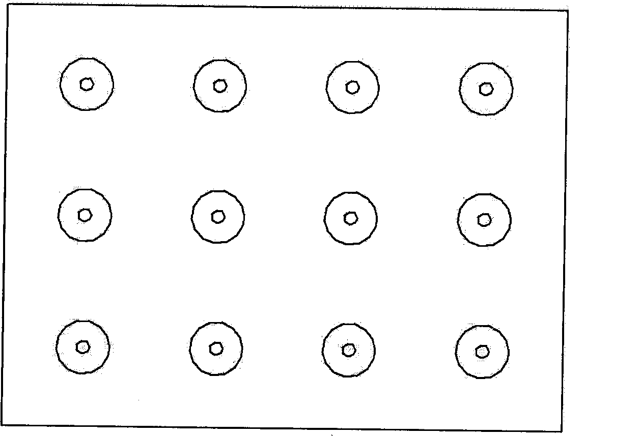
[0035] (2) Substrate etching step: use KW-4A glue homogenizer (Research Department of Microelectronics Center of Chinese Academy of Sciences) 2 A layer of BP218 positive photoresist (Beijing Chemical Reagent Research Institute) was coated on the layer, and photolithography was carried out with a 1# mask (the model of the photolithography machine used was Karl Suss MA6), and then developed on the photoresist The pattern of the micropit array was made on the surface; then, using the remaining photoresist layer as a mask, dilute HF solution (HF:H 2 O=1:7) etch away the exposed SiO 2 , the remaining SiO 2 layer is used as a mask layer for etching the silicon substrate; etching Si uses TMAH (tetramethylammonium hyd...

Embodiment 2

[0056] (1) Preparation steps: grow a layer of SiO on the surface of a 2-inch silicon wafer by thermal oxidation 2 layer with a thickness of 20nm, thoroughly cleaned with acetone and deionized water, and baked on a hot plate at 200°C for 10 minutes to completely dry;

[0057] (2) Substrate etching step: use KW-4A glue homogenizer (Research Department of Microelectronics Center of Chinese Academy of Sciences) 2 A layer of BP218 positive photoresist (Beijing Chemical Reagent Research Institute) was coated on the layer, and photolithography was carried out with a 1# mask (the model of the photolithography machine used was Karl Suss MA6), and then developed on the photoresist The pattern of the micropit array was made on the surface; then, using the remaining photoresist layer as a mask, dilute HF solution (HF:H 2 O=1:7) etch away the exposed SiO 2 , the remaining SiO 2 layer is used as a mask layer for etching the silicon substrate; etching Si uses TMAH (tetramethylammonium hyd...

Embodiment 3

[0068] (1) preparation step, (2) substrate etching step, (3) pretreatment step, (4) glue leveling step, (5) exposure step and (6) development step are completely the same as in Example 1;

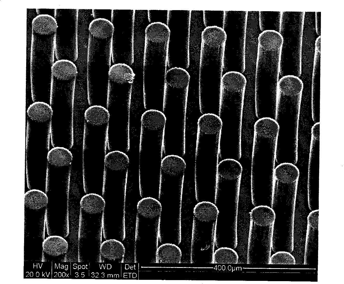
[0069] (7) Pyrolysis step: Put the post-baked silicon substrate into a GSL-1400X vacuum tube furnace (Luoyang Weida High Temperature Instrument Co., Ltd.), and gradually increase the temperature for three times for pyrolysis to obtain high aspect ratio carbon. microelectromechanical devices. The specific process is:

[0070] (7-1) Vacuuming, the vacuum degree reaches 10 -3 Tor, the purpose is to release oxygen to prevent the photoresist structure from being burned;

[0071] (7-2) Nitrogen gas is introduced at 2000 milliliters per minute (sccm) under standard conditions, the purpose is to further discharge excess oxygen;

[0072] (7-3) Rise from room temperature to 300°C at a heating rate of 3°C / min, keep warm for 20min, and continue to feed nitrogen at 2000sccm; this process is to furthe...


PUM

PropertyMeasurementUnit
Sheet resistanceaaaaaaaaaa
Resistivityaaaaaaaaaa

Abstract

The invention relates to a method for preparing a carbon micro electromechanical device with high depth-to-width ratio, belongs to a method for preparing a carbon micro structural device, and solves the problems that the micro electromechanical device with high depth-to-width ratio prepared by the prior method has complex process and high cost and is easy to separate from a substrate. The method comprises: (1) a preparation step; (2) a substrate etching step; (3) a pretreatment step; (4) a glue evening step, (5) an exposure step; (6) a development step; and (7) a pyrolysis step. The method combines photoetching and pyrolysis of thick glue to obtain the carbon micro electromechanical device with the high depth-to-width ratio applied to a micro electromechanical system, and has the characteristics of simple process, fine patterns, firm structure, no special requirement on equipment, and low cost; and the prepared device has high combination strength with the substrate and long service life, and can be used as an microelectrode applied to the MEMS fields such as micro battery, biological chip, micro electrochemical sensor, and the like.

Description

technical field [0001] The invention belongs to a preparation method of a carbon microstructure device, in particular to a preparation method of a carbon microelectromechanical device with a high aspect ratio. Background technique [0002] In recent years, the application of carbon materials in microelectromechanical systems (MEMS) has attracted the attention of many scholars at home and abroad. Carbon is a very common and special element in nature, such as diamond, graphite, coke, glassy carbon, and buckyballs (C60) with special structures, as well as carbon nanotubes and carbon nanofibers that have attracted much attention recently. Both are forms of carbon. Because of this, carbon materials are widely used in the fields of physics, chemistry, mechanics, thermals, and electronics. The selection of carbon materials is another innovation in materials since the development of MEMS for decades. The advantages of carbon materials are significant. It has a more perfect lattic...

Claims


Application Information

Patent Timeline
IPC IPC(8): B81C1/00G03F7/16G03F7/20G03F7/32
Inventor 汤自荣史铁林马伟龚杰廖广兰聂磊
Owner HUAZHONG UNIV OF SCI & TECH
Why Eureka
Try Eureka