Crystalline silicon solar battery

A technology of solar cells and crystalline silicon, applied in the field of solar cells, can solve the problems of low conversion efficiency, lower cell conversion efficiency, increase recombination loss, etc., and achieve the effect of small recombination loss

Inactive Publication Date: 2009-10-21
黄麟
View PDF1 Cites 19 Cited by
  • Summary
  • Abstract
  • Description
  • Claims
  • Application Information

AI Technical Summary

Problems solved by technology

Taking the crystalline silicon solar cell with a junction depth of 250nm using the above-mentioned patented technology (hereinafter referred to as the patented cell) as an example, due to the use of a high-conductivity transparent conductive film, when the grid line density is the minimum (0.5 lines/cm), its blocking The loss is about 4.5% lower than that of the usual crystalline silicon solar cells, that is, the patented cell will absorb 4.5% more photons, and the junction depth of 250nm means that the n-type diffusion layer in the patented cell will absorb 10.6% of the photons. A photon can only produce a pair of electron-hole pairs at most, that is, the number of photons directly corresponds to the number of electron-hole pairs, and the recombination loss caused by the front electrode of the transparent conductive film in the patented battery will make almost all of these absorbed Photons become useless, therefore, removing the number of photons absorbed due to reduced shading

Method used


Image

  • Crystalline silicon solar battery
  • Crystalline silicon solar battery
  • Crystalline silicon solar battery

Examples


specific Embodiment approach 1

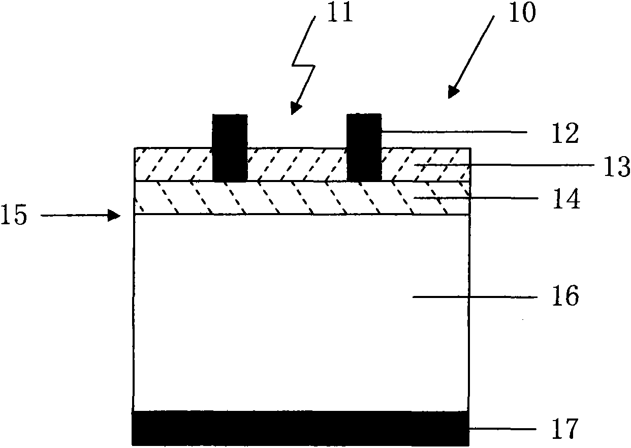
[0049] Follow the steps below to get figure 2 Shown is the p-type crystalline silicon solar cell of the present invention.

[0050] 1. Provide p-type crystalline silicon wafers, whose doping concentration is 4×10 15 ~4×10 16 / cm 3 within range.

[0051] 2. Carry out chemical polishing in a solution containing sodium hydroxide.

[0052] 3. On the back of the p-type crystalline silicon wafer (optional on both surfaces) form a p + Type heavily doped layer, requiring its impurity concentration to be greater than 10 20 / cm 3 , the junction depth is ≥2 μm, and the dopant material can be boron (B).

[0053] 4. The p on the back of the p-type crystalline silicon wafer + A layer of SiO is deposited on the heavily doped layer by atmospheric pressure chemical vapor deposition (APCVD) or low pressure chemical vapor deposition (LPCVD) 2 film, its thickness is required to be greater than 0.5 μm.

[0054] 5. First, use photoresist to coat the p on the back of the p-type crystal s...

Embodiment 1

[0063] If the same silicon material as the usual industrial production of crystalline silicon solar cells is used, that is, oriented p-type monocrystalline silicon wafers with a thickness of 0.2mm at the CZ level, the selected process parameters are: resistance of p-type monocrystalline silicon wafers The ratio is about 1Ωcm; the positive n + type doped layer, its thickness is about 100nm, and its doping concentration is about 5×10 19 / cm 3 ; The window layer can be ZnO:Al thin film, its square resistance is about ≤100Ω / □, and its thickness is about 150nm; the distance between the metal grid lines of the front grid-shaped metal electrodes is 2.85mm. Then the conversion efficiency of the battery can reach about 17%, which is about 6% higher than the industrialized average level of common crystalline silicon solar cells.

Embodiment 2

[0065] If the same silicon material as the usual industrial production of crystalline silicon solar cells is used, that is, oriented p-type monocrystalline silicon wafers with a thickness of 0.2mm at the CZ level, the selected process parameters are: resistance of p-type monocrystalline silicon wafers The ratio is about 1Ωcm; the positive n + type doped layer, its thickness is about 10nm, and its doping concentration is about 6×10 18 / cm 3 ; The window layer can be ZnO:Al thin film, its square resistance is about ≤100Ω / □, and its thickness is about 150nm; the distance between the metal grid lines of the front grid-shaped metal electrodes is 2.85mm. Then the conversion efficiency of the cell can reach about 17.8%, which is about 11% higher than the industrialized average level of common crystalline silicon solar cells.


PUM

PropertyMeasurementUnit
Thicknessaaaaaaaaaa
Sheet resistanceaaaaaaaaaa
Resistivityaaaaaaaaaa

Abstract

The invention discloses a crystalline silicon solar battery which comprises a grid metal electrode 22 at the front face, a window layer 23, a second conduction type heavily doped layer 24, a first conduction type lightly doped crystalline silicon substrate 26 and an electrode 27 at the back face in turn. Provided with the second conduction type heavily doped layer 24 which is thin enough and is thick enough in doping density, the invention can lower the recombination loss caused by the window layer 23, provided with the window layer 23, the invention can lower the ohmic loss caused by the second conduction type heavily doped layer 24 which is thin enough and is thick enough in doping density and simultaneously lower the sheltering loss caused by the grid metal electrode 22 at the front face, thereby enabling the transfer efficiency of a usual crystalline silicon solar battery to be enhanced by at least more than 10 percent.

Description

technical field [0001] The invention relates to a solar cell, in particular to a crystalline silicon (single crystal silicon or polycrystalline silicon) solar cell. Background technique [0002] Currently, common crystalline silicon solar cells 10, such as figure 1 As shown, its typical structure includes: front grid metal electrode 12, anti-reflection and passivation layer 13, n + type heavily doped layer 14, p-type lightly doped crystalline silicon substrate 16, and a back electrode 17, wherein the front gate-like metal electrode 12 is directly connected to the n + Type heavily doped layer 14 is connected and forms an ohmic contact; n + Type heavily doped layer 14 is formed on one surface of p-type lightly doped crystalline silicon substrate 16 by methods such as diffusion, ion implantation or epitaxy, and, n + Type heavily doped layer 14 and p-type lightly doped crystalline silicon substrate 16 form a homogeneous p-n junction, and form a p-n junction depletion region (...

Claims


Application Information

Patent Timeline
IPC IPC(8): H01L31/068H01L31/06
CPCY02E10/50
Inventor 黄麟
Owner 黄麟
Why Eureka
Try Eureka