

Graded zinc diffusing method based on MOCVD (Metal-Organic Chemical Vapor Deposition) system for producing chip of indium-gallium-arsenic photoelectric detector
A photodetector and diffusion method technology, applied in circuits, electrical components, semiconductor devices, etc., to achieve good uniformity, suitable for mass production, and good process repeatability
- Summary
- Abstract
- Description
- Claims
- Application Information
AI Technical Summary
Problems solved by technology
Method used
Image

Examples
Embodiment Construction
[0025] The applicant found the following points in the research:
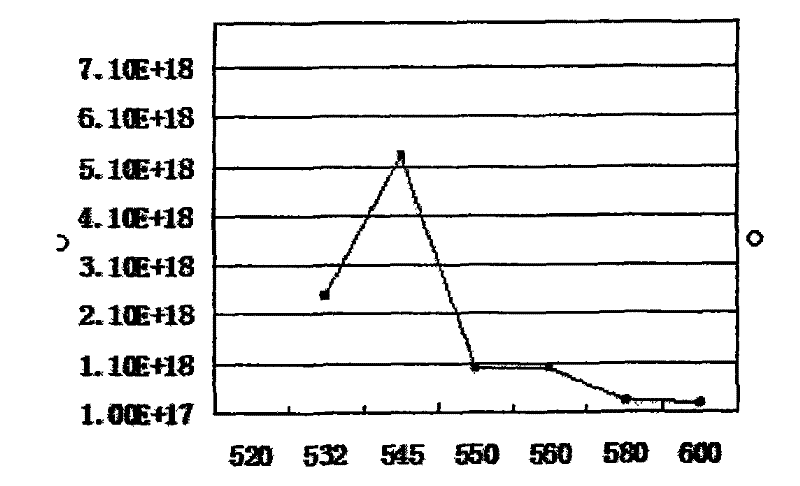
[0026] 1. There is a big difference in the diffusion law of zinc in InP and InGaAs materials. It is easy to diffuse in InP materials, but the diffusion rate of zinc in InGaAs materials is slow.
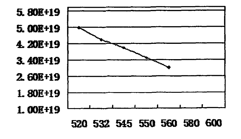
[0027] 2. There is a certain limit to the diffusion depth. For detectors with InGaAs PIN structure, the InGaAs layer needs to have a higher carrier concentration, but the zinc at this flow rate has oversaturated the InP layer, which will cause adverse effects, and between InP and InGaAs The interface formed by the material is not clear enough, and it is easy to accumulate too many charged particles at the junction of the InP and InGaAs interface.
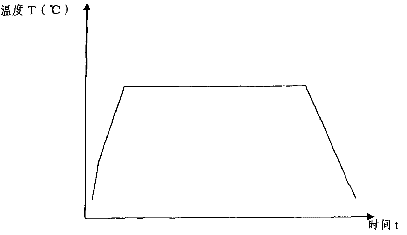
[0028] In order to make both InP and InGaAs materials obtain higher carrier concentrations and clear PN junction interfaces, the applicant accurately calculated the diffusion time of each layer of materials, and when the InP layer with a certain thickness is diffused and ent...
PUM
 Abstract
Description
Claims
Application Information