Process for preparing silicon dioxide nano-cone array

A silicon dioxide and nanocone technology, applied in nanostructure manufacturing, nanotechnology, nanotechnology, etc., can solve the problems of expensive instruments, difficult to achieve large-area construction, and low efficiency.

Inactive Publication Date: 2010-04-14
JILIN UNIV
View PDF0 Cites 30 Cited by
  • Summary
  • Abstract
  • Description
  • Claims
  • Application Information

AI Technical Summary

Problems solved by technology

Electron beam (E-Beam) etching and focused ion beam (FIB) etching can accurately control parameters such as the period and bottom diameter of the nanocone array, ...

Method used


Image

  • Process for preparing silicon dioxide nano-cone array
  • Process for preparing silicon dioxide nano-cone array
  • Process for preparing silicon dioxide nano-cone array

Examples


Embodiment 1

[0063] 1. The preparation method of polystyrene microspheres:

[0064] Under nitrogen protection, with 40 milliliters of absolute ethanol and 100 milliliters of deionized water as the dispersion medium, 3.3 milliliters of styrene, 0.0733 grams of potassium persulfate, and 0.0807 grams of sodium dodecylsulfonate were added to the In the reactor of the mechanical stirrer and the reflux condenser, the mechanical stirring speed was 350 rpm. The polymerization reaction was carried out in a water bath at 70° C., and after 10 hours of reaction, a stable milky white emulsion of monodisperse polystyrene microspheres was obtained, and the diameter of the microspheres was 210 nanometers.

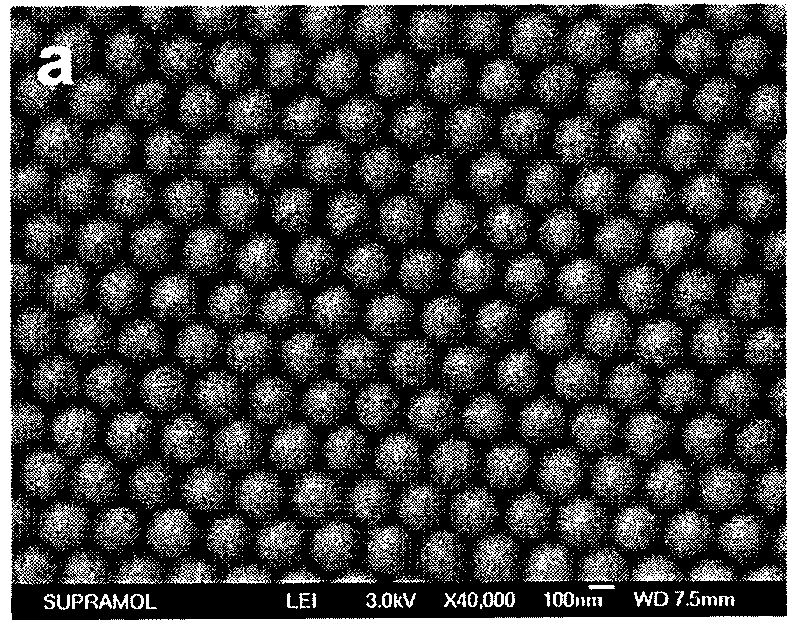
[0065] 2. Preparation of polystyrene monolayer colloidal crystals:

[0066] The prepared polystyrene microspheres were centrifuged and washed, and then dispersed with a mixed solution of absolute ethanol and deionized water with a volume ratio of 1.5:1 to obtain a monodisperse polystyrene microsphere ...

Embodiment 2

[0070] 1. The preparation method of polystyrene microspheres and the preparation method of polystyrene monolayer colloidal crystals are shown in Example 1.

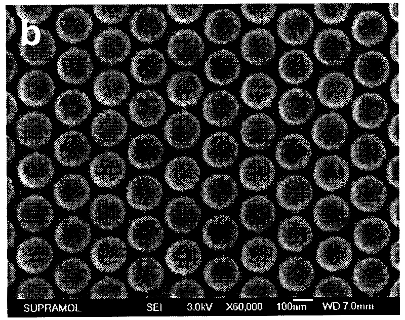
[0071] 2. Preparation of silica nanocone arrays:

[0072] Reactive ion etching of fluorine was carried out on the quartz substrate of the obtained surface-mounted polystyrene monolayer colloidal crystal, the etching power was RF 300W, the chamber pressure was 40mTorr, the flow rate of tetrafluoromethane was 30SCCM, and the flow rate of argon gas was 20SCCM , the etching time was 4 minutes, and then the remaining polystyrene was removed with chloroform to obtain a silica nanocone array with a period of 210 nm, a height of 211 nm, and a bottom diameter of 196 nm, as shown in Figure 5.

Embodiment 3

[0074] 1. The preparation method of polystyrene microspheres and the preparation method of polystyrene monolayer colloidal crystals are shown in Example 1.

[0075] 2. Preparation of silica nanocone arrays:

[0076]Reactive ion etching of fluorine was carried out on the quartz substrate of the obtained surface-mounted polystyrene monolayer colloidal crystal, the etching power was RF 300W, the chamber pressure was 40mTorr, the flow rate of tetrafluoromethane was 30SCCM, and the flow rate of argon gas was 20SCCM , the etching time was 3 minutes, and then the remaining polystyrene was removed with chloroform to obtain a silica nanocone array with a period of 210 nm, a height of 190 nm, and a bottom diameter of 201 nm, as shown in Figure 6.


PUM

PropertyMeasurementUnit
Diameteraaaaaaaaaa
Thicknessaaaaaaaaaa
Bottom diameteraaaaaaaaaa

Abstract

The invention relates to a process for preparing a silicon dioxide nano-cone array which has large area, controllable interval, controllable cycle and sequential arrangement, and is directly fabricated on a substrate. The process includes three steps: cleaning the quartz plate substrate and performing hydrophilic process on the surface of the quartz plate substrate; preparing polystyrene single-layer colloidal crystals; fabricating the silicon dioxide nano-cone array. The silicon dioxide nano-cone array prepared by the process has extremely excellent wide-band anti-reflection and transmission increasing properties, can realize effectively reducing surface reflection loss and increasing light transmission from ultraviolet light to visible light (350nm to 800 nm) and then to the inside of middle-infrared-band (800nm to 2.5 micrometer) by controlling the cycle. Simultaneously, by changing nature of the surface of nano-cones, antifogging and super-hydrophobic surfaces can be fabricated. The process is simple, comparatively controllable and has wide application prospect on photoelectric devices with low cost and large area and on fabrication of anti-reflection surfaces.

Description

technical field [0001] The invention relates to a method for preparing a silicon dioxide nanocone array, in particular to a method for directly constructing a silicon dioxide nanocone array with a large area, a controllable distance, a controllable period and an orderly arrangement on a substrate. Background technique [0002] Quartz is a widely used window material, but part of the light is lost due to the reflection of light on the surface, which affects the light transmittance and reduces the performance of optical components. The usual method is to build an anti-reflection and anti-reflection coating on the surface of the optical element to increase the light transmittance and improve the performance of the element. This anti-reflection coating can improve the efficiency of solar cells; it can eliminate the phenomenon of "ghost image", so it has wide application prospects. At present, the method of preparing anti-reflection and anti-reflection coatings in industry is th...

Claims


Application Information

Patent Timeline
IPC IPC(8): B82B3/00B81C1/00
Inventor 杨柏李云峰张俊虎朱守俊贾菲
Owner JILIN UNIV
Why Eureka
Try Eureka