Device and method for controlling residual stress on surface of metal microstructure

A metal microstructure and residual stress technology, applied in metal processing equipment, manufacturing tools, laser welding equipment, etc., can solve the problems of inability to realize online detection and judgment of laser shot peening strengthening effect, affect service life, etc., and achieve improved mechanical properties , the effect of improving the service life

Inactive Publication Date: 2010-06-09
JIANGSU UNIV
View PDF1 Cites 17 Cited by
  • Summary
  • Abstract
  • Description
  • Claims
  • Application Information

AI Technical Summary

Problems solved by technology

For the microstructure manufacturing technology, it is mainly the microstructure forming process, such as silicon micromachining, LIGA, high energy beam etching, micro-EDM and micro-stamping, etc. During the production process, residual tensile stress is often generated on the surface of the microstructure. Affect the service life
[0003] A.H.Clauer and B.P.Fairand of Battlells Columbus Laboratory in the United States proposed in the patent U.S.4401477 "Laser shock processing" to irradiate the surface of parts with high-energy short-pulse laser to generate strong shock waves and form residual compressive stress in the surface layer to improve The method of mechanical properties of parts, but the laser shot peening method described in this patent is non-controllable, it cannot realize the online detection and judgment of the laser sh

Method used


Image

  • Device and method for controlling residual stress on surface of metal microstructure
  • Device and method for controlling residual stress on surface of metal microstructure
  • Device and method for controlling residual stress on surface of metal microstructure

Examples


Embodiment

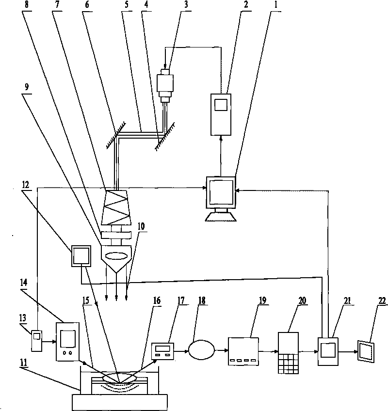
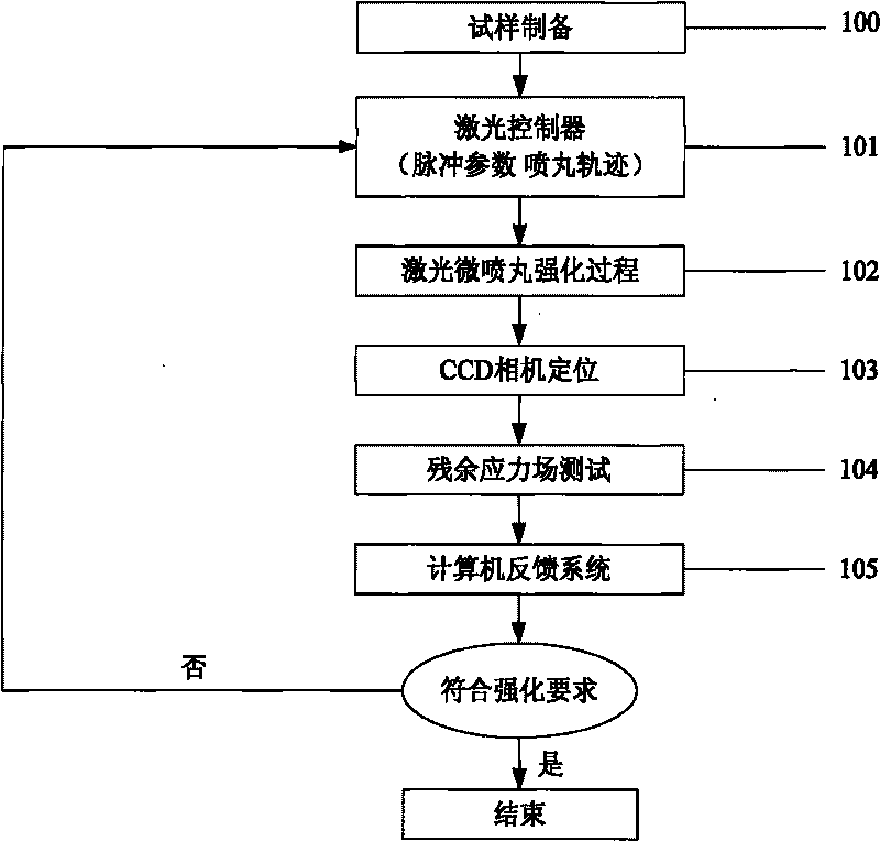
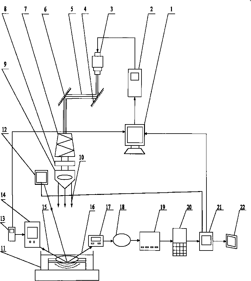
[0023] Take the aluminum sample as an example, place the aluminum sample on figure 1 In the measuring box 11, press figure 1 The structure connects the laser micro shot peening system, measurement feedback system and control system, such as figure 2 As shown, the implementation process is as follows:

[0024] [1] Step 100: Cover an energy absorbing layer (10μm thick aluminum foil) and a constraining layer (1mm thick water curtain) on the surface of the aluminum film; complete sample preparation:

[0025] [2] Step 101: Set and adjust the output laser parameters: the spot size is 25μm, the pulse width is 6ns, the energy is 0.8mJ, the spot overlap rate is 50%, and the shot blasting path is programmed according to the size of the processing area.

[0026] [3] Step 102: Start the numerical control system to control the laser shot peening head 9, and perform impact treatment on the surface of the micro component with a linear track;

[0027] [4] Step 103: the aluminum film with the substra...


PUM


Abstract

The invention discloses a device and a method for controlling the residual stress on the surface of a metal microstructure. A laser micro shot blasting generation system and a measuring feedback system are respectively connected with a control system; a pulse laser beam is focused on an area to be subjected to shot blasting on the surface of a workpiece; incident X rays emitted by a synchronous accelerating irradiation light source enter a measurement box, are diffracted by the surface of the workpiece and then are received by a detector; electric pulse is amplified by an amplifier and enters a pulse height analyzer; signal pulse is transmitted to a counter, processed by a microcomputer and fed back to a computer control system by the microcomputer for error analysis and parameter correction; and a charge Coupled device (CCD) optical camera is used for positioning and monitoring a processing area on the surface of the workpiece. The invention effectively controls the residual stress on the surface of the metal microstructure, improves the mechanical properties of the metal micro component, prolongs the service life of the metal micro component, and enables the surface of the metal micro component to generate the residual pressure stress with the depth up to over 20mu m and the pressure ranging from -120 to -100MPa.

Description

Technical field [0001] The invention relates to the field of microstructure surface treatment of micro-electromechanical systems and laser technology applications, in particular to a method and device for controlling the level of residual stress on the surface of metal microstructures, and is particularly suitable for the surface treatment of metal microcomponents with a thickness of 100-200 μm. Background technique [0002] At present, metal microstructures and microdevices with specific functional material properties are increasingly used in microsystems or embedded in conventional machines as intelligent core components. As a load-bearing component, micro-devices are usually subjected to alternating loads such as heat and force, resulting in their deformation, fracture, wear and fatigue damage, causing failure of the microstructure, resulting in the failure of the entire micro-electromechanical system and machine. The wear resistance and fatigue performance of the steel put fo...

Claims


Application Information

Patent Timeline
IPC IPC(8): B23K26/00C21D10/00C22F3/00
Inventor 周建忠王敏黄舒樊玉杰卫登辉
Owner JIANGSU UNIV
Why Eureka
Try Eureka