Gallium and indium doped single crystal silicon material for solar battery and preparation method thereof

A solar cell and monocrystalline silicon technology, which is applied in polycrystalline material growth, single crystal growth, single crystal growth, etc., can solve the problems of solar cells that are prone to light decay, and achieve moderate strength, less crystal defects, and low light decay Effect

Active Publication Date: 2010-08-18
LONGI GREEN ENERGY TECH CO LTD
View PDF0 Cites 30 Cited by
  • Summary
  • Abstract
  • Description
  • Claims
  • Application Information

AI Technical Summary

Problems solved by technology

[0011] The purpose of the present invention is to provide a gallium-indium-doped monocrystalline silicon material for solar cells, which solves the problem that the existing boron-doped monocrystalline silicon materials are prone to light decay when preparing solar cells

Method used


Image

  • Gallium and indium doped single crystal silicon material for solar battery and preparation method thereof
  • Gallium and indium doped single crystal silicon material for solar battery and preparation method thereof
  • Gallium and indium doped single crystal silicon material for solar battery and preparation method thereof

Examples


Embodiment 1

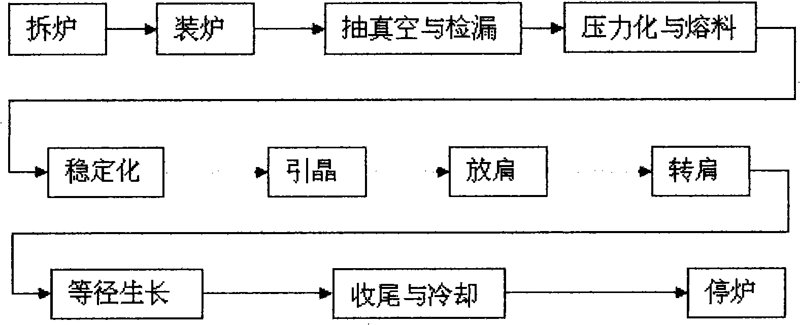
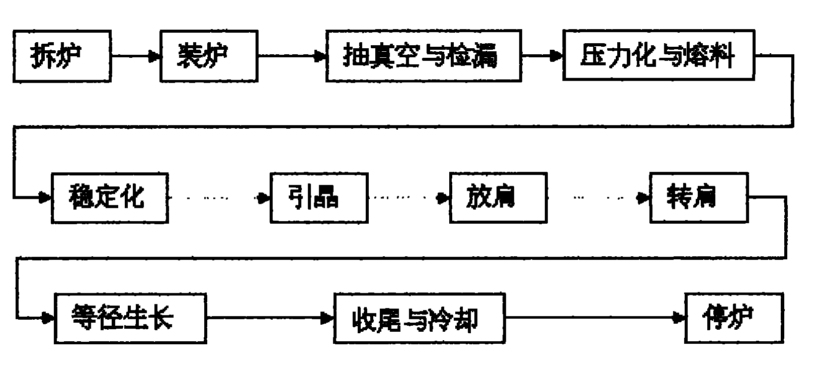
[0072] Step 1: Disassemble the furnace according to the conventional method and clean the furnace.

[0073] Step 2: Load the furnace. According to the number of atoms per cubic centimeter of single crystal silicon material, weigh 1.0 × 10 14 atoms / cm 3 Gallium, 5.0 x 10 12 atoms / cm 3 Indium, the rest is monocrystalline silicon, first spread the weighed monocrystalline silicon all over the bottom of the quartz crucible, and then put the weighed gallium and indium on the monocrystalline silicon in the quartz crucible, preferably on quartz In the central part of the crucible, more monocrystalline silicon is then placed in the quartz crucible, so that the added monocrystalline silicon completely covers the added high-purity gallium and indium, and the quartz crucible is placed in the monocrystalline furnace.

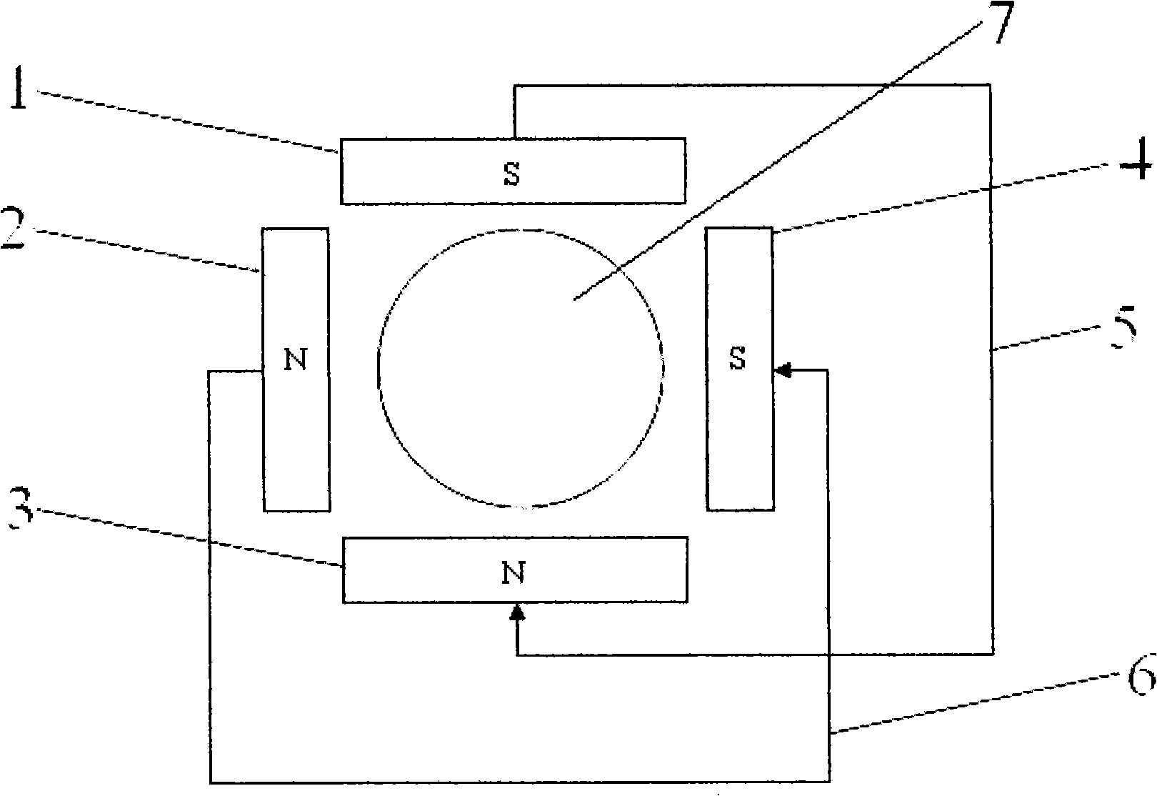
[0074] And, the magnetic field is arranged outside the single crystal furnace, and the specific implementation is carried out according to the following steps: outside t...

Embodiment 2

[0085] Step 1: Disassemble the furnace according to the conventional method and clean the furnace.

[0086] Step 2: Load the furnace. According to the number of atoms per cubic centimeter of single crystal silicon material, weigh 1.0 × 10 18 atoms / cm 3 Gallium, 5.0 x 10 16 atoms / cm 3 Indium, the rest is monocrystalline silicon, first spread the weighed monocrystalline silicon all over the bottom of the quartz crucible, and then put the weighed gallium and indium on the monocrystalline silicon in the quartz crucible, preferably on quartz In the central part of the crucible, more monocrystalline silicon is then placed in the quartz crucible, so that the added monocrystalline silicon completely covers the added high-purity gallium and indium, and the quartz crucible is placed in the monocrystalline furnace.

[0087] And, the magnetic field is arranged outside the single crystal furnace, and the specific implementation is carried out according to the following steps: outside t...

Embodiment 3

[0098] Step 1: Disassemble the furnace according to the conventional method and clean the furnace.

[0099] Step 2: Load the furnace. According to the number of atoms per cubic centimeter of single crystal silicon material, weigh 3.03×10 15 atoms / cm 3 Gallium, 8.3 x 10 12 atoms / cm 3 The indium and the rest are single crystal silicon, and the silicon crystal with high concentration of gallium-doped or gallium-doped indium is obtained by drawing through the cz furnace; then, the silicon crystal is broken, mixed with the single crystal silicon and added to the quartz crucible, and the quartz crucible is placed in the single crystal crucible. inside the furnace.

[0100] And, the magnetic field is arranged outside the single crystal furnace, and the specific implementation is carried out according to the following steps: outside the conventional single crystal furnace, two sets of perpendicular permanent magnets fixed with yoke plates are arranged along the two radial directio...


PUM

PropertyMeasurementUnit
electrical resistivityaaaaaaaaaa
diameteraaaaaaaaaa
conversion efficiencyaaaaaaaaaa

Abstract

The invention discloses a gallium and indium doped single crystal silicon material for a solar battery, which consists of the following components according to atom number per cubic centimeter of the single crystal silicon material: 1.0X10<14> to 1.0X10<18> gallium, 5.0X10<12> to 5.0x10<16> indium and the balance of single crystal silicon. The invention also discloses a method for preparing the gallium and indium doped single crystal silicon material for the solar battery, which is implemented by the following steps of: dismantling a furnace by using a regular method, cleaning a hearth and assembling the furnace; vacuumizing the inside of a single crystal furnace and detecting the leakage of the single crystal furnace by using a regular method; pressuring materials and smelting the materials; stabilizing the melt; seeding crystals; performing shouldering; performing shoulder rotation; performing isodiametric growth; performing ending and cooling the obtained product; and stopping the furnace. The gallium and indium doped single crystal silicon material for the solar battery has the advantages of high conversion efficiency, low light attenuation, low oxide content in the single crystal silicon and uniform radial distribution in a single crystal silicon rod; and the preparation method of the invention effectively controls the thermal conversion of silicon melt and grows the high-quality gallium and indium doped single crystal silicon material for the solar battery.

Description

technical field [0001] The invention belongs to the technical field of monocrystalline silicon for solar energy, and specifically relates to a gallium-indium-doped monocrystalline silicon material for solar cells, and also relates to a preparation method of the monocrystalline silicon material. Background technique [0002] Due to the easy availability of silicon materials and the relatively mature production methods of solar-grade high-purity silicon, silicon crystal (monocrystalline silicon, polycrystalline silicon) solar cells have been widely used as an important type of clean energy. Into the 21st century, the use of such batteries has grown tremendously. [0003] At present, monocrystalline silicon for solar cells generally chooses a single doped boron element, that is, boron-doped monocrystalline silicon. For this kind of boron-doped single crystal silicon, the CZ method (Czochralski, 1918), which is convenient and easy to produce and the resistivity distribution of ...

Claims


Application Information

Patent Timeline
Patent Type & Authority Applications(China)
IPC IPC(8): C30B29/06C30B15/00C30B15/04
CPCC30B29/06C30B15/00
Inventor 张群社
Owner LONGI GREEN ENERGY TECH CO LTD
Why Eureka
Try Eureka