Method for making gradational diffusion photoelectric diode by using MOCVD epitaxial system

A photodiode, gradient type technology, applied in circuits, electrical components, final product manufacturing, etc., can solve the problems of large dark current, nonlinear distortion of optical signal detection, inability to make unilateral abrupt junctions and low-ohmic contacts, etc. Small dark current, small capacitance reliability, and the effect of improving chip responsivity and response rate

Active Publication Date: 2010-12-15
WUHAN HUAGONG GENUINE OPTICS TECH
View PDF5 Cites 3 Cited by
  • Summary
  • Abstract
  • Description
  • Claims
  • Application Information

AI Technical Summary

Problems solved by technology

Traditional fabrication of photodetector cores usually adopts open tube diffusion or closed tube diffusion method, and the doping concentration reaches 1E18cm -3, , cannot make single-sided abrupt junctions and low-ohm contacts; and traditional planar or mesa-type dies have the disadvantages of nonlinear distortion of optical signal detection or large dark current

Method used


Image

  • Method for making gradational diffusion photoelectric diode by using MOCVD epitaxial system
  • Method for making gradational diffusion photoelectric diode by using MOCVD epitaxial system
  • Method for making gradational diffusion photoelectric diode by using MOCVD epitaxial system

Examples


Embodiment Construction

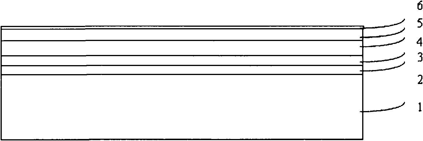
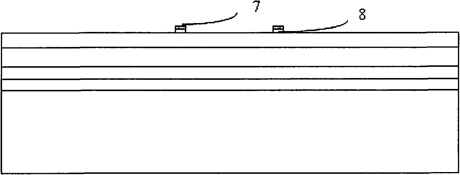
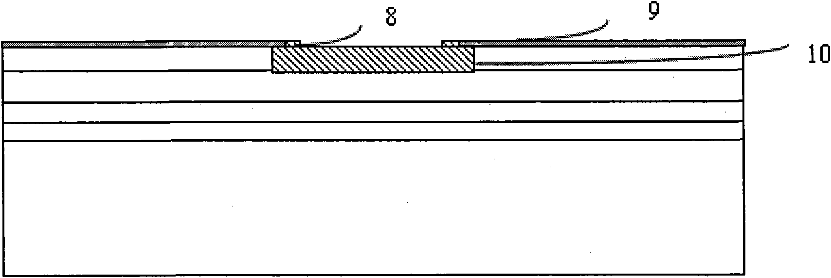
[0036] The present invention adopts the MOCVD epitaxy system to carry out primary epitaxy of the photodiode on the semi-insulating indium phosphide substrate, forms the indium gallium arsenic ohmic contact layer, adopts the gradient diffusion method based on the MOCVD epitaxy system for doping, and adopts reactive ion etching ( RIE) combined with chemical wet etching method to make quasi-mesa, use chemical wet etching method to make the second step, make S i o 2 Passivation layer, making photosensitive surface, evaporation etching electrode, substrate thinning, back sputtering and electrode alloying.

[0037] The present invention will be described in detail below with reference to the accompanying drawings.

[0038] The primary epitaxy of the photodiode is carried out on the semi-insulating indium phosphide substrate by MOCVD method, and the epitaxy is composed of five layers (see figure 1 ), from bottom to top are Fe-doped semi-insulating indium phosphide I substrate 1, 0....


PUM

PropertyMeasurementUnit
thicknessaaaaaaaaaa
breaking strengthaaaaaaaaaa
yield strengthaaaaaaaaaa

Abstract

The invention relates to a method for making a gradational diffusion photoelectric diode by using an MOCVD epitaxial system. The method comprises the following steps performed on a semi-insulating indium phosphide substrate by using the MOCVD epitaxial system: performing the primary epitaxy of the photoelectric diode; forming an indium gallium arsenide ohmic contact layer; doping by using an MOCVD epitaxial system-based gradational diffusion method; making a pseudo-table by using a method combining reactive ion etching and chemical wet etching; making a second step by using a chemical wet etching method; making a SiO2 passivation layer and a photosensitive surface; evaporating an etching electrode; thinning the substrate and performing back sputtering and electrode alloying. Zinc phosphide is continuously generated during the diffusion and the method has the advantages of high doping, low ohmic contact resistance and high responsibility; moreover, abrupt junctions are formed during the diffusion, the dark current is small and the reliability is good; the gradational diffusion is adopted, which is implemented by two steps and is uniform; besides, the pseudo-table structure is adopted, the dark current is small, the reliability is good and the dark current of a chip is only 10pA.

Description

technical field [0001] The invention relates to a method for manufacturing a high-speed photodiode used in an optical communication system, in particular to a method for manufacturing a quasi-mesa and coplanar electrode type high-speed indium gallium arsenic / indium phosphide photodiode based on MOCVD system gradient diffusion. Background technique [0002] The advancement of informatization and the demand for network applications rapidly promote the development of network technology. Driven by the rapid increase of the total bandwidth of the network at the rate of doubling every year, new network applications and network technologies are constantly emerging. The development and maturity of new technologies such as dense wavelength division multiplexing (DWDM) technology, passive optical network (PON) technology, Ethernet (Ethernet) technology, and long-term evolution (TD-LTE) technology have made optical communication technology move towards large-capacity, Development of h...

Claims


Application Information

Patent Timeline
Patent Type & Authority Applications(China)
IPC IPC(8): H01L31/18C23C16/44
CPCY02P70/50
Inventor 唐琦秦龙吴瑞华
Owner WUHAN HUAGONG GENUINE OPTICS TECH
Why Eureka
Try Eureka