Polysilicon film low-temperature physical vapor deposition device and method thereof

A physical vapor deposition, polysilicon thin film technology, applied in vacuum evaporation plating, coating, sputtering and other directions, can solve the problems of reducing production cost, low production efficiency, high cost, improving competitiveness and avoiding cost High and low cost effect

Inactive Publication Date: 2012-11-28
DALIAN UNIV OF TECH +1
View PDF3 Cites 0 Cited by
  • Summary
  • Abstract
  • Description
  • Claims
  • Application Information

AI Technical Summary

Problems solved by technology

The problem with this method is that it uses the toxic gas silane (SiH 4 ) needs to be equipped with complete gas recovery equipment and systems, resulting in higher costs. In addition, its growth rate is low, which is not conducive to reducing production costs
[0008] The above-mentioned direct generation preparation methods have the following problems in varying degrees: all have been applied to the H 2 Diluted SiH 4 gas as source gas, SiH 4 It is a colorless, flammable and toxic gas, which determines that it needs to be equipped with a complete set of exhaust gas treatment auxiliary equipment and systems
This method is tedious and cumbersome due to indirect growth.
Its production efficiency is not high, so it is not conducive to industrial promotion

Method used


Image

  • Polysilicon film low-temperature physical vapor deposition device and method thereof
  • Polysilicon film low-temperature physical vapor deposition device and method thereof
  • Polysilicon film low-temperature physical vapor deposition device and method thereof

Examples


Embodiment 1

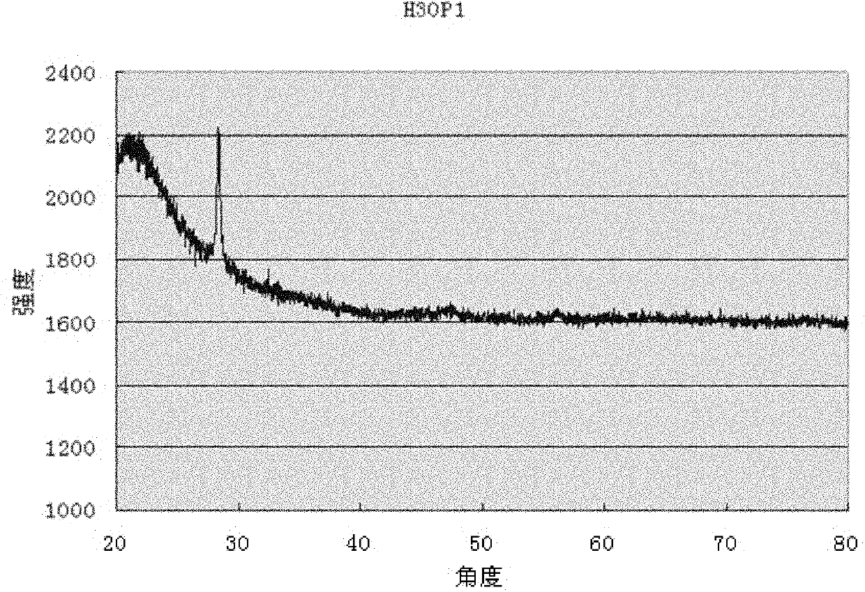
[0041] Example 1 Preparation of Polysilicon Thin Film Sample No. H30P1 and Characteristic Test

[0042] Step 1: Sample Preparation

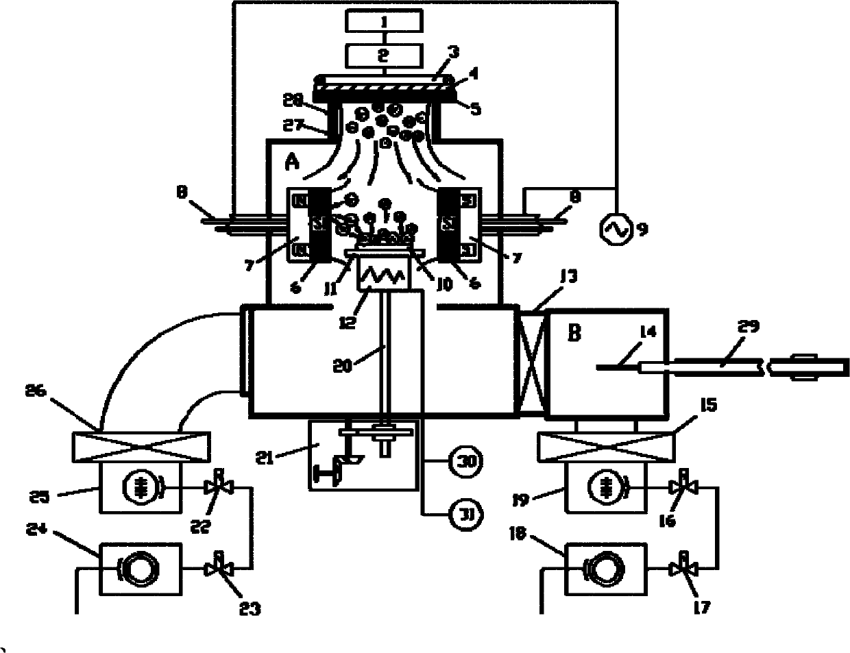
[0043] Prepare sample 10: monocrystalline silicon silicon wafer with a diameter of φ100mm, quartz wafer with a diameter of 100mm and ordinary glass wafer with a diameter of 100mm; load it on the sample tray 11 of the auxiliary vacuum chamber B, and evacuate the auxiliary vacuum chamber B until the specified pressure value is reached Open the flapper valve 13 connecting the auxiliary vacuum chamber B and the main vacuum chamber A, and transfer the sample 10 to the main vacuum chamber A through the magnetic transfer rod 29 and the sample pallet fork 14;

[0044] Step 2: Pre-treatment of sample preparation

[0045] The background pressure of the main vacuum chamber A is pumped to a high vacuum of 2.0*10 -5 pa, the sample 10 is preheated to about 200°C, firstly, Ar is introduced into the main vacuum chamber A, and the air pressure reaches 1 Pa, the...

Embodiment 2

[0054] Example 2 Preparation of Polysilicon Thin Film Sample No. B0H30P1 and Characteristic Test

[0055] Step 1: sample preparation (with step 1 in Example 1);

[0056] Step 2: Pre-treatment of sample preparation

[0057] The background pressure of the main vacuum chamber A is pumped to a high vacuum of 2.0*10 -5 pa, sample 10 is preheated to about 200°C, here the Ar bombardment step is not implemented, and H is directly injected into the main vacuum chamber A 2 The mixed gas with Ar, the flow ratio is 90sccm / 30sccm, the pressure value reaches 1Pa, and the ICP uses the power of 1500w to continuously discharge the mixed gas for 40 seconds, thus forming H 2 Mixed gas plasma with Ar, and give the sample a bias voltage of 10-100V, where the measured bias current is 0.03A, and sample 10 is subjected to pre-deposition treatment;

[0058] Step 3: Sample preparation and deposition

[0059] Into the main vacuum chamber A, the H with a flow ratio of 60sccm / 90sccm 2 Mix the gas wit...

Embodiment 3

[0064] Example 3 Preparation of Polysilicon Thin Film Sample No. H30P1ICP8 and Characteristic Test

[0065] Step 1: Sample preparation;

[0066] Step 2: Pretreatment of sample preparation (step 1 and step 2 are the same as step 1 and step 2 in Example 2);

[0067]Step 3: Sample preparation and deposition

[0068] Into the main vacuum chamber A, the H with a flow ratio of 60sccm / 90sccm 2 Mix the gas with Ar, adjust the second slide valve 26, and set the pressure value to 1Pa. Turn on the ICP inductively coupled plasma source, the ICP power is 800w, no bias is applied to the sample 10 here, and the DC pulse magnetron sputtering twin target is turned on, the power is 200w, and the deposition time is 50 minutes;

[0069] Step 4: post-processing of sample preparation;

[0070] Step 5: Take out the sample (step 4 and step 5 are the same as step 4 and step 5 in Example 1).

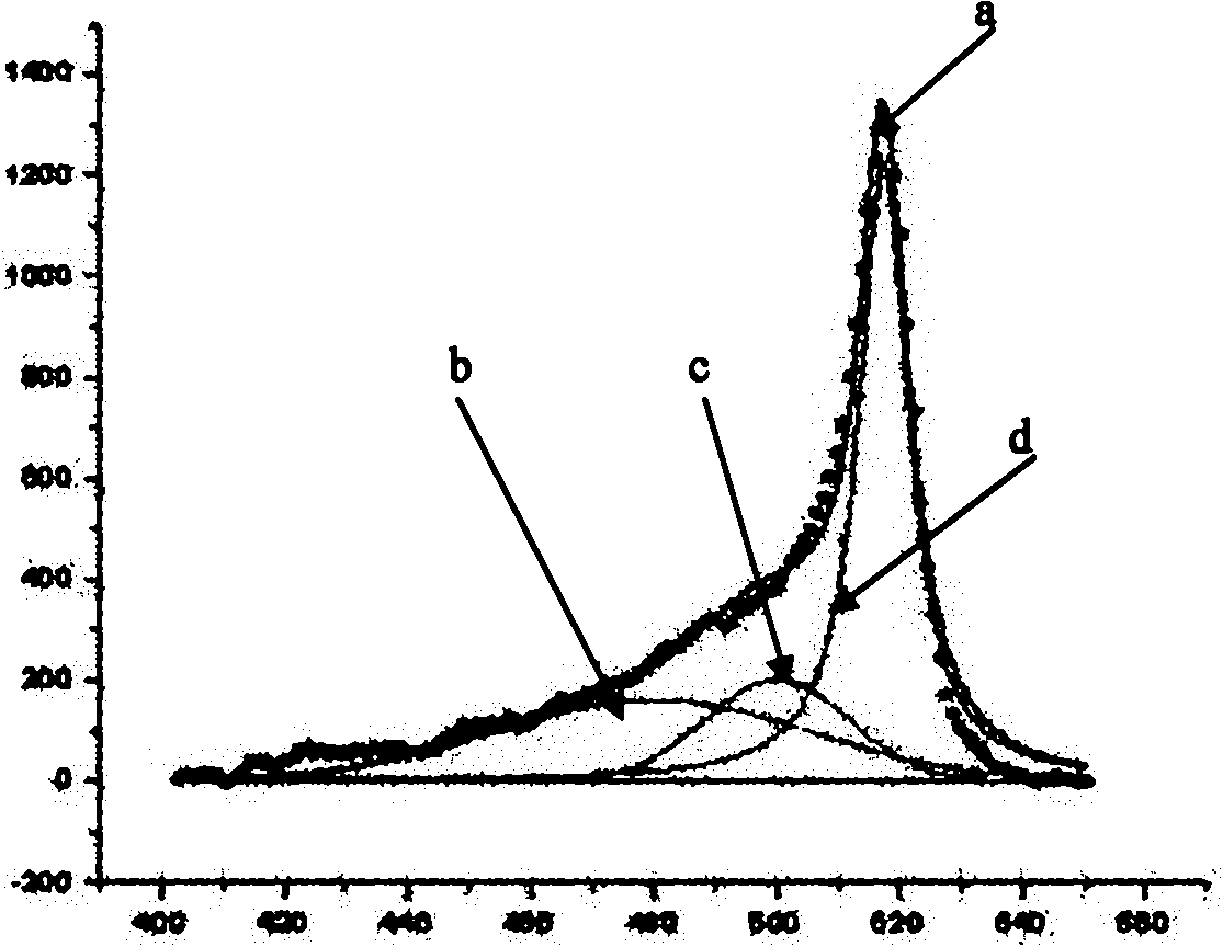
[0071] X-ray diffractometer (Cu K α Radiation, λ=0.15406nm) for structural analysis of the prepared film...


PUM

PropertyMeasurementUnit
diameteraaaaaaaaaa
diameteraaaaaaaaaa
diameteraaaaaaaaaa

Abstract

The invention relates to a polysilicon film low-temperature physical vapor deposition device and a method thereof, belonging to the technical field of semiconductor materials. By the deposition device and the method thereof, the low-temperature polysilicon film of which the host crystal orientation is (111), the grain diameter is tens of nanometers, and the proportion of the polysilicon part exceeds 80% can be generated by the steps of sample preparation, pretreatment for sample preparation, deposition, post-treatment, sample taking and the like. The physical vapor deposition method is substituted for the current plasma enhanced chemical vapor deposition technology, and the polysilicon film is directly deposited under the precondition of not using SiH gas. Because the substrate (simple glass) with low cost has a lower melting point, the polysilicon film can be directly deposited on the simple glass substrate under the condition of relatively low temperature (less than 300 DEG C), thusavoiding the defect of high cost of the formerly used substrate, and greatly improving the competitiveness.

Description

technical field [0001] The invention relates to a low-temperature physical vapor deposition device and method for polysilicon thin films, more specifically, a reactive magnetron sputtering device and method with plasma source assistance, and belongs to the technical field of semiconductor thin film materials. Background technique [0002] As a new material, polysilicon thin film has been widely used in thin film transistor (TFT) display, semiconductor storage, solar energy and other fields. Polysilicon thin films have attracted more and more attention due to their high electron mobility and stable optical properties. Polysilicon thin film has photosensitivity in the long-wave band, can effectively absorb visible light and has light stability, unlike a-Si:H has light degradation (SW) effect, so polysilicon thin film can be used as a more efficient and stable photovoltaic thin film material. At the same time, the mobility of polysilicon film can reach 300cm 2 ·V -1 ·s -1 T...

Claims


Application Information

Patent Timeline
Patent Type & Authority Patents(China)
IPC IPC(8): C23C14/14C23C14/35
Inventor 苏元军孙琦高桥英治董闯徐军范鹏辉
Owner DALIAN UNIV OF TECH
Why Eureka
Try Eureka