
Method for preparing high-performance surface acoustic wave device with multilayer film structure

A surface acoustic wave device, multi-layer film technology, applied in coating, metal material coating process, ion implantation plating and other directions, can solve the problems of inability to withstand high power, unstable product quality, unfavorable promotion and application, etc. It is conducive to large-scale popularization and application, significant production practical significance, and convenient and easy process conditions.

Inactive Publication Date: 2011-06-15
TIANJIN UNIVERSITY OF TECHNOLOGY
View PDF3 Cites 4 Cited by
  • Summary
  • Abstract
  • Description
  • Claims
  • Application Information

AI Technical Summary

Problems solved by technology

[0003] Conventional SAW materials (such as quartz, lithium niobate LiNbO 3 , zinc oxide ZnO, etc.), the surface acoustic wave phase velocity is low (both lower than 4000m / s), and the SAW device with a frequency of 2.5GHz is made with it, and the finger width d of the interdigital transducer (IDT) must be less than 0.4μm The IDT finger width d corresponding to a SAW device with a frequency of 5 GHz is less than 0.2 μm, which is already approaching the limit of the current semiconductor industry level. This problem seriously restricts the further improvement of the frequency of SAW devices; moreover, the transmitter (TX) filter of the mobile communication system filters high-power signals, such a thin IDT finger width d, large resistance, will generate a large number of Heat dissipation, coupled with the low thermal conductivity of these conventional SAW materials, so they cannot withstand high power, which makes it difficult for SAW devices made of the above conventional SAW materials to meet the requirements of high-frequency and / or high-power mobile communications
At present, in the high-performance multi-layer thin-film structure surface acoustic wave devices, the adhesion between each layer of film is poor, resulting in unstable product quality, which is not conducive to large-scale promotion and application, etc.

Method used


Image

  • Method for preparing high-performance surface acoustic wave device with multilayer film structure
  • Method for preparing high-performance surface acoustic wave device with multilayer film structure
  • Method for preparing high-performance surface acoustic wave device with multilayer film structure

Examples


Embodiment 1

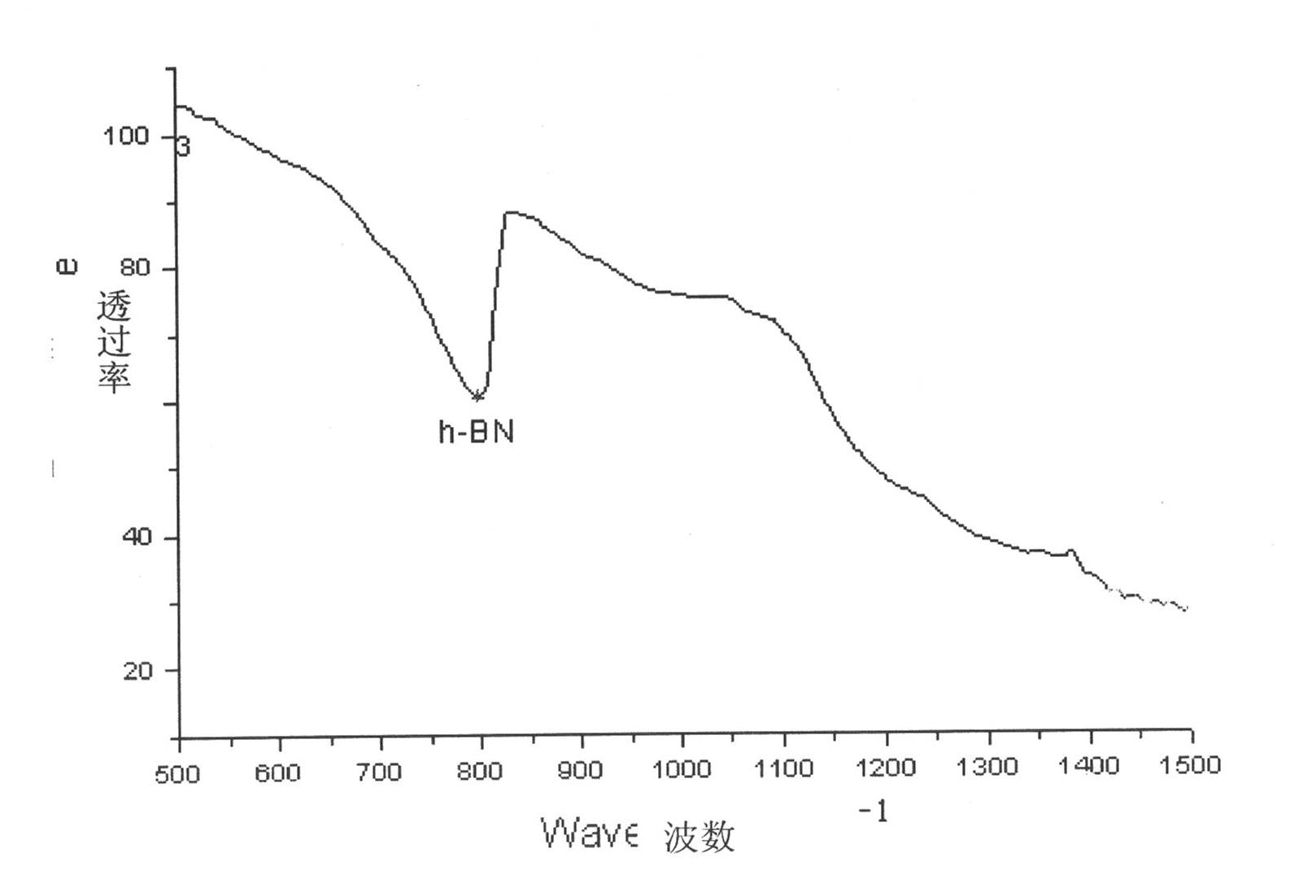
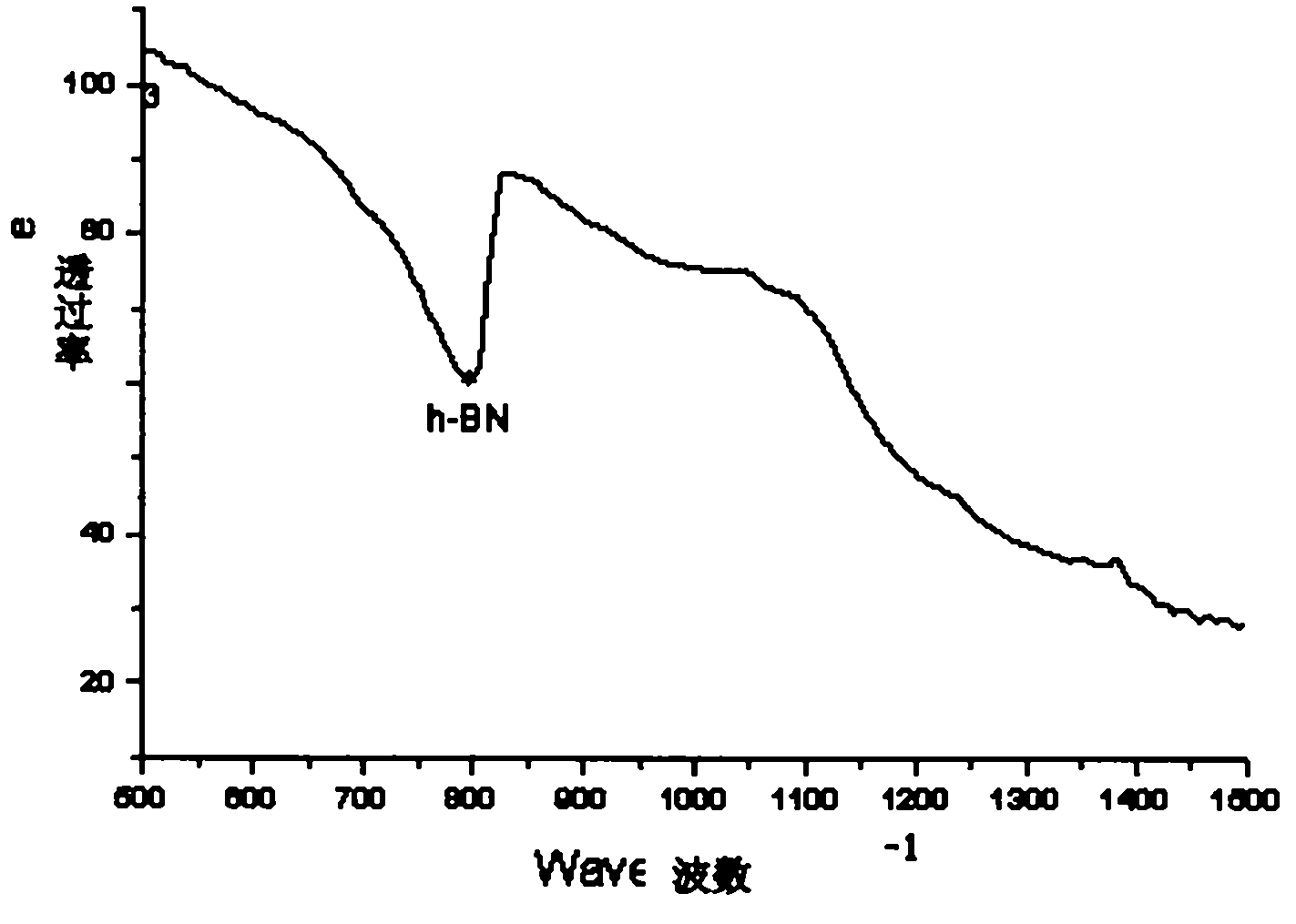
[0020] Firstly, a high-performance multilayer thin-film structure surface acoustic wave device is prepared according to the existing technology, that is, a layer of h-BN film is formed by sputtering on the surface of the CVD diamond film, and finally a high-performance multilayer thin-film structure surface acoustic wave device is obtained, specifically including The following steps:

[0021] 1) polishing the surface of the chemical vapor deposition CVD diamond film to form a mirror-polished CVD diamond film surface, the preparation steps are:

[0022] First, on a mirror-polished silicon substrate, in a mixed atmosphere composed of argon, hydrogen, and methane, the volume ratio between the argon, hydrogen, and methane is 70%:27%:3%, and in the deposition chamber , the microwave power is 5000W, the deposition chamber pressure is 80 Torr, the mixed gas flow rate is 600sccm (milliliters per minute) and the substrate temperature is 750°C, and the chemical vapor deposition is carri...

Embodiment 2

[0040] The steps of preparing a high-performance multilayer thin film structure surface acoustic wave device according to the prior art are the same as those in Example 1.

[0041] In this embodiment, a layer of h-BN film was sputtered on the surface of the mirror-polished and hydrogen-terminated CVD diamond film using an ultra-high vacuum radio frequency magnetron sputtering system. The sputtering power used was 230W, and the substrate temperature was The temperature is 400°C, the working pressure is 1.1Pa, the mass flow ratio between argon and nitrogen is 20:4, and it is prepared by the following steps:

[0042] 1) Depositing a B-rich boron nitride bottom layer. During the sputtering process, the working gas in the vacuum sputtering chamber is a mixed gas of argon and nitrogen, the flow rate of argon gas is fixed at 20 sccm, and the flow rate of nitrogen gas is increased from 1 sccm to 4 sccm, and the step increment value is 1 sccm per step, argon gas and nitrogen gas The v...


PUM

PropertyMeasurementUnit
thicknessaaaaaaaaaa
thicknessaaaaaaaaaa
thicknessaaaaaaaaaa

Abstract

The invention discloses a method for preparing a high-performance surface acoustic wave device with a multilayer film structure. In the invention, a substrate is a CVD (Chemical Vapor Deposition) diamond film, and the surface of the CVD diamond film forms a layer of h-BN (hexagonal boron nitride) film. The film is deposited by adopting a vacuum sputtering method, and the substrate of the film is a mirror polishing silicon substrate. The crystal face index is 100, the base pressure of a vacuum sputtering room is 5X10⁻⁴Pa, and the target material for sputtering is hot-pressed h-BN with purity of 99.99%, wherein the hot-pressed h-BN with purity of 99.99% comprises the preparation steps of: depositing a boron nitride underlayer rich in B, then changing the negative bias value of the substrate from 0V to 100V, and finally prolonging the sputtering deposition time to 80 minutes under the condition of keeping process conditions unchanged. Compared with the prior art, the method has the advantages that the equipment used in the preparation method is simple, the process conditions are convenient and easy, and the preparation method is beneficial to large-scale application and has important significance in both production and practice.

Description

technical field [0001] The invention relates to the technical field of surface acoustic wave devices, in particular to a preparation method of a high-performance multilayer film structure surface acoustic wave device. Background technique [0002] In recent years, the rapid development of mobile communication has made radio communication frequency band a limited and precious natural resource. For mobile communication systems, the frequency band below 1GHz has been fully occupied (the first generation digital system); the frequency of the second generation digital system is from 900MHz to 1.9GHz; in the third generation digital system, the global roaming frequency range is 1.8~2.2GHz, the satellite positioning system (GPS) frequency is 1.575GHz, and the application frequency range of low earth orbit new satellite communication (LEO) is 1.6GHz~2.5GHz. Therefore, the application frequency of the current mobile communication system is getting higher and higher , there is an urg...

Claims


Application Information

Patent Timeline
Patent Type & Authority Applications(China)
IPC IPC(8): C23C14/35C23C14/06C23C14/02
Inventor 薛玉明杨保和祝俊刚辛志军狄海荣武长强
Owner TIANJIN UNIVERSITY OF TECHNOLOGY
Learn More