

Crystalline silicon solar cell and preparation method thereof
A technology of solar cells and crystalline silicon, applied in circuits, photovoltaic power generation, electrical components, etc., can solve the problems of expensive photolithography technology, complex process, unfavorable mass production, etc., achieve improved anti-reflection performance, simple preparation process, passivation excellent chemical effect
- Summary
- Abstract
- Description
- Claims
- Application Information
AI Technical Summary
Problems solved by technology
Method used
Image

Examples
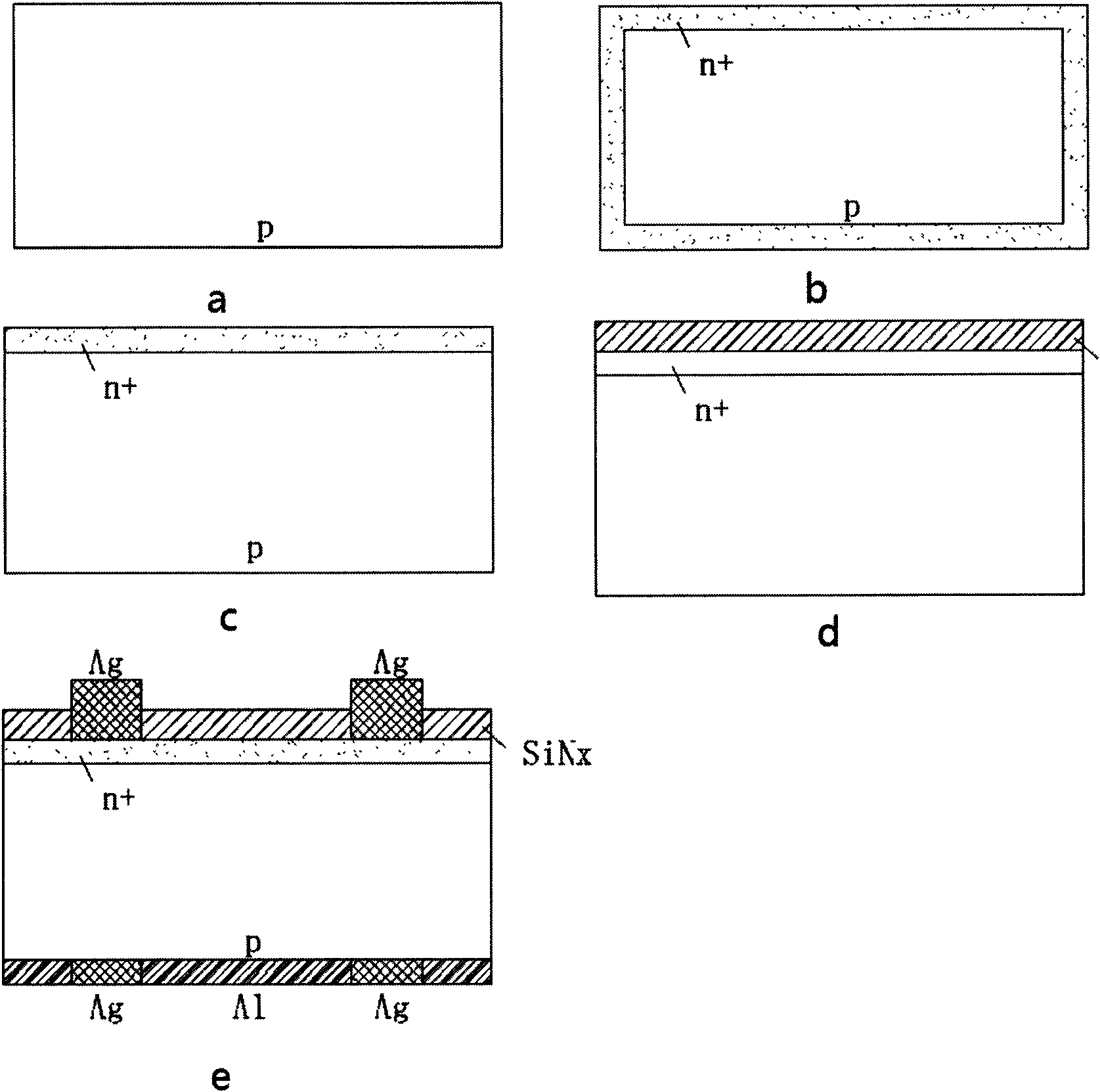
Embodiment 1
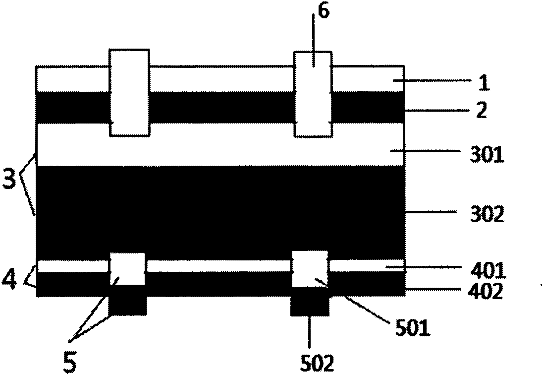
[0038] like image 3 Shown, a crystalline silicon solar cell structure. Its preparation process is as follows:
[0039] 1. Remove p-type silicon substrate surface damage, acid or alkali texturing to form anti-reflection structure and chemical cleaning;
[0040] 2. Diffusion in POCl3 atmosphere and removal of peripheral pn junction and phosphosilicate glass by etching to form pn+ structure;
[0041] 3. Soak the p-type substrate surface for 30 minutes in a mixed solution with a volume ratio of HNO3:H2O2=10:1; wherein the concentration of HNO3 is 68%, and the concentration of H2O2 is 30%;
[0042] 4. The silica sol prepared by the sol-gel method, the steps are as follows:
[0043] a Under strong stirring, pour aluminum isopropoxide into boiling water containing part of nitric acid for hydrolysis, and keep stirring; after 30 minutes, the temperature drops to 90°C.
[0044] b Add concentrated nitric acid after 60 minutes to obtain clarified alumina sol, and cool naturally;
[...
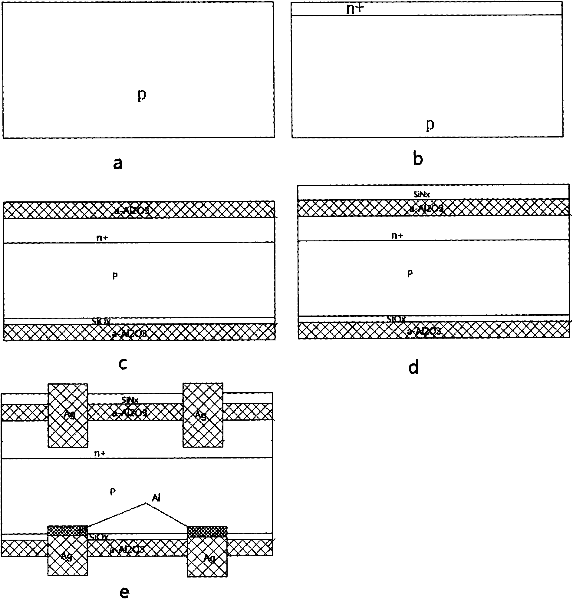
Embodiment 2
[0050] Same as in Example 1, except that the spin coating method is used to prepare the amorphous alumina layer, the thickness of the amorphous alumina film on the surface of the n+ emitter is 10 nm, and the film thickness of the composite passivation medium layer on the surface of the p-type substrate is 50 nm.
PUM
| Property | Measurement | Unit |
|---|---|---|
| thickness | aaaaa | aaaaa |
| thickness | aaaaa | aaaaa |
| thickness | aaaaa | aaaaa |
Abstract
Description
Claims
Application Information