

Square silicon nanometer hole and preparation method thereof
A silicon nano and hole technology, applied in the field of nano materials, can solve the problems of high cost, complex process, long process cycle, etc., and achieve the effect of improving efficiency, low cost and wide application prospect.
- Summary
- Abstract
- Description
- Claims
- Application Information
AI Technical Summary
Problems solved by technology
Method used
Image

Examples
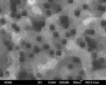
Embodiment 1
[0031] Shake the cut monocrystalline silicon wafer with acetone and alcohol for 10 minutes and 5 minutes respectively, then treat it with a mixed solution of sulfuric acid and hydrogen peroxide with a volume ratio of 4:1 at 80°C for 1 hour to remove heavy metal ions on the surface, and finally Treat with a mixed solution of hydrogen peroxide: ammonia water: water = 1:1:3 (volume ratio) at 80°C for 1 hour. A silver film with a thickness of about 10 nm was vacuum evaporated on the cleaned silicon wafer. Put the silver-coated silicon wafer into a tube-type high-temperature furnace, anneal with 95 sccm argon as the protective gas, the temperature is 300°C, and the holding time is 60 minutes. Immerse the annealed silicon wafer with silver particles in the corrosion solution of hydrofluoric acid and hydrogen peroxide, wherein the concentration of hydrofluoric acid is 2.3-3.2 mol / L, the concentration of hydrogen peroxide is 0.2-0.38 mol / L, and the reaction temperature is 55°C , the ...
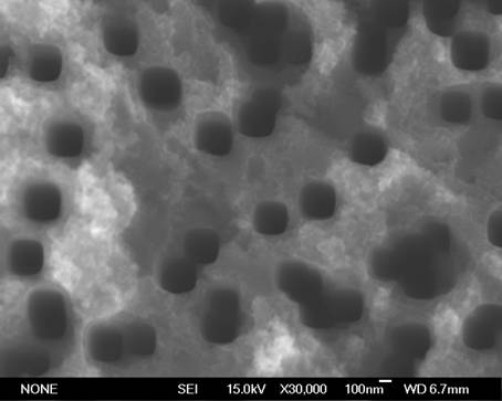
Embodiment 2
[0033] Shake the cut monocrystalline silicon wafer with acetone and alcohol for 10 minutes and 5 minutes respectively, then treat it with a mixed solution of sulfuric acid and hydrogen peroxide with a volume ratio of 4:1 at 80°C for 1 hour to remove heavy metal ions on the surface, and finally Treat with a mixed solution of hydrogen peroxide: ammonia water: water = 1:1:3 (volume ratio) at 80°C for 1 hour. A silver film with a thickness of about 8 nm was vacuum evaporated on the cleaned silicon wafer. Put the silver-coated silicon wafer into a tube-type high-temperature furnace, anneal with 95 sccm argon as the protective gas, the temperature is 300°C, and the holding time is 90 minutes. Immerse the annealed silicon wafer with silver particles in the corrosion solution of hydrofluoric acid and hydrogen peroxide, wherein the concentration of hydrofluoric acid is 3.2-4.0 mol / L, the concentration of hydrogen peroxide is 0.38-0.4 mol / L, and the reaction temperature is 65°C , the c...
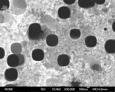
Embodiment 3
[0035]Shake the cut monocrystalline silicon wafer with acetone and alcohol for 10 minutes and 5 minutes respectively, then treat it with a mixed solution of sulfuric acid and hydrogen peroxide with a volume ratio of 4:1 at 80°C for 1 hour to remove heavy metal ions on the surface, and finally Treat with a mixed solution of hydrogen peroxide: ammonia water: water = 1:1:3 (volume ratio) at 80°C for 1 hour. A silver film with a thickness of about 6 nm was vacuum evaporated on the cleaned silicon wafer. Put the silver-coated silicon wafer into a tube-type high-temperature furnace, anneal with 95 sccm argon as the protective gas, the temperature is 300°C, and the holding time is 90 minutes. Immerse the annealed silicon wafer with silver particles in the corrosion solution of hydrofluoric acid and hydrogen peroxide, wherein the concentration of hydrofluoric acid is 3.2-3.6 mol / L, the concentration of hydrogen peroxide is 0.3-0.38 mol / L, and the reaction temperature is 55°C , the co...
PUM
| Property | Measurement | Unit |
|---|---|---|
| thickness | aaaaa | aaaaa |
| depth | aaaaa | aaaaa |
| depth | aaaaa | aaaaa |
Abstract
Description
Claims
Application Information