LED (Light-Emitting Diode) structure and manufacturing method thereof

A technology of LED structure and micro-nano structure, applied in semiconductor devices, electrical components, circuits, etc., can solve the problems of limited vertical structure LED application, low vertical structure LED yield, poor bonding process compatibility, etc., to improve light extraction. Efficiency, low price, effect of improving adhesion

Inactive Publication Date: 2011-09-14
PEKING UNIV
View PDF5 Cites 8 Cited by
  • Summary
  • Abstract
  • Description
  • Claims
  • Application Information

AI Technical Summary

Problems solved by technology

The usual reflective layer is a metal with high reflectivity such as Ag, Al layer or multi-layer metal composite structure. However, the metal characteristics of Ag, Al, etc. determine the poor compatibility between the preparation process of the reflective layer and the bonding process, resulting in low yield of vertical structure LEDs. However, mass production cannot be achieved, which limits the application of vertical structure LEDs

Method used


Image

  • LED (Light-Emitting Diode) structure and manufacturing method thereof
  • LED (Light-Emitting Diode) structure and manufacturing method thereof
  • LED (Light-Emitting Diode) structure and manufacturing method thereof

Examples


Embodiment 1

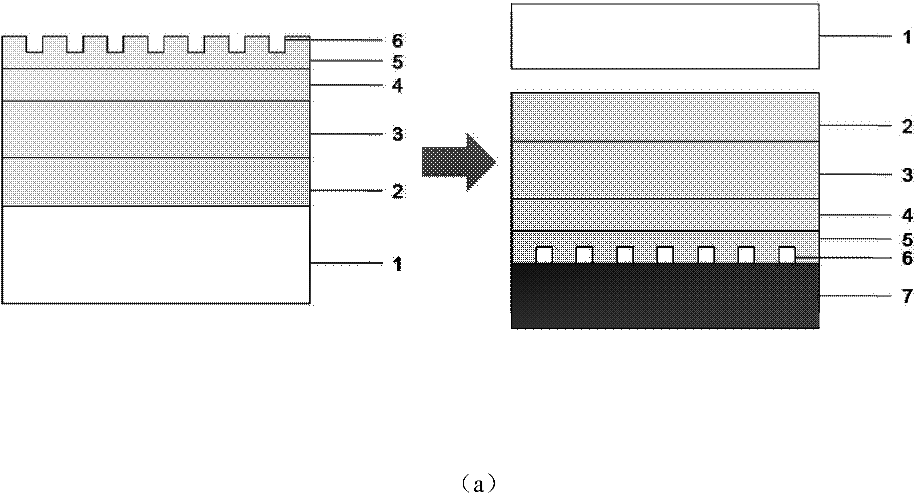
[0020] Embodiment 1: GaN-based blue LED chip with high-power vertical structure (or ordinary flip-chip structure) with periodic micro-nano structure on the transparent electrode surface

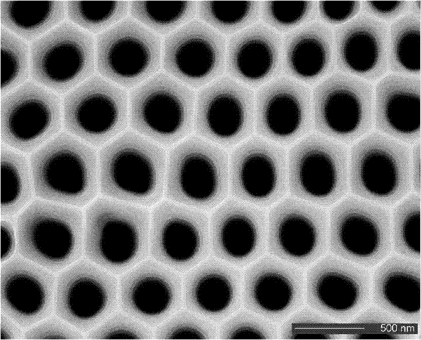
[0021] 1. Put the electropolished aluminum foil into a phosphoric acid solution, and prepare a periodic micro-nano-structured AAO film with a period of about 460 nm by secondary anodic oxidation. Remove the aluminum substrate with a saturated copper chloride solution, and then expand the pores with a 5% phosphoric acid solution to obtain a periodic micro-nano structure AAO template with a pore diameter of about 270 nm, such as figure 1 shown.

[0022] 2. Grow a GaN-based blue LED structure with a luminous wavelength of about 460nm on a sapphire substrate, and implement a conventional LED process to obtain an LED wafer with a transparent electrode layer (ITO or Ni / Au, etc.) on p-GaN. The steps 1. The prepared AAO film with periodic micro-nano structure is evenly and tightly adhered to the sur...

Embodiment 2

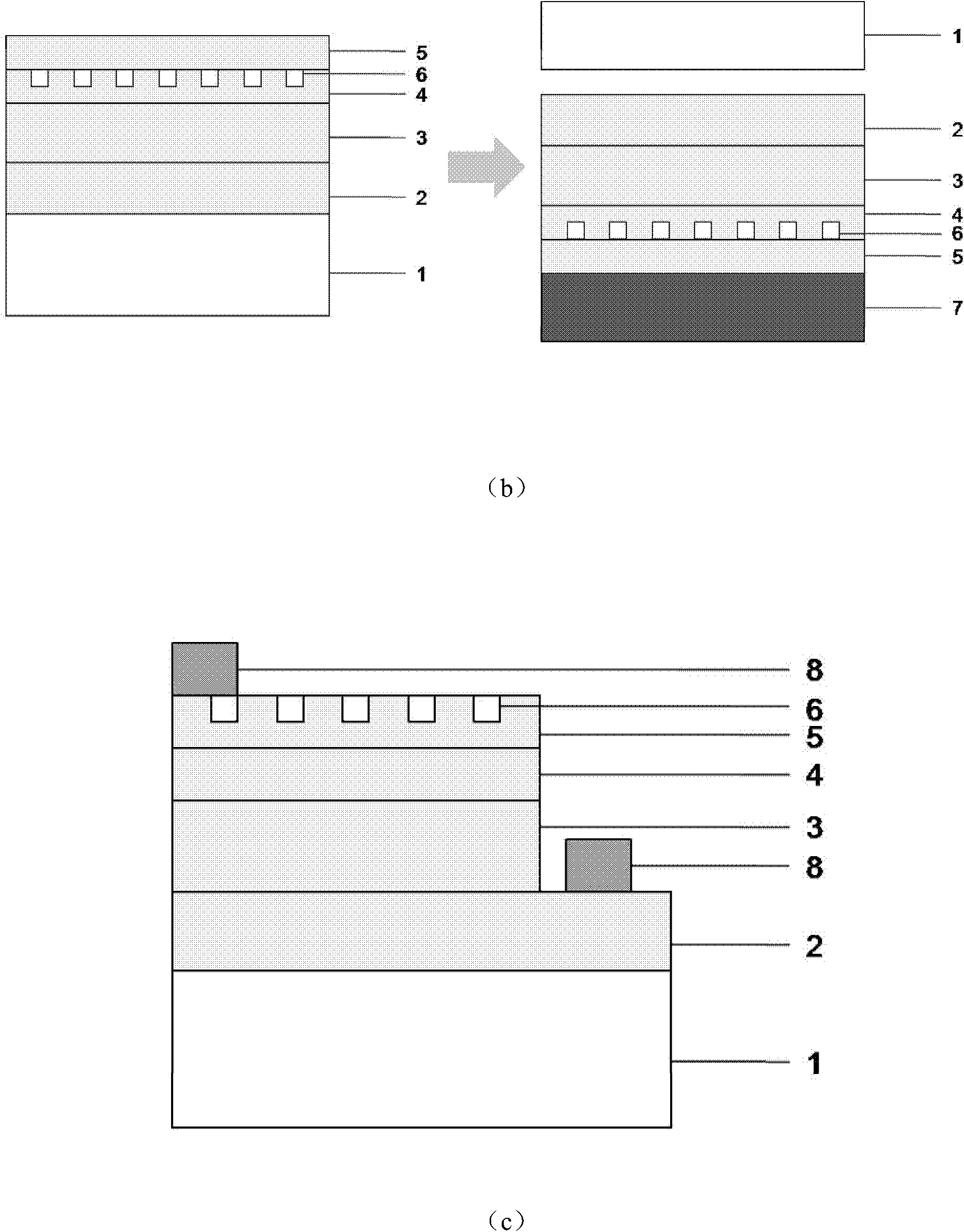
[0026] Embodiment 2: a high-power vertical structure (or ordinary flip-chip structure) GaN-based blue LED chip with a periodic micro-nano structure on the surface of p-GaN

[0027] 1. the first step of the present embodiment is the same as the first step of embodiment one, on this basis:

[0028] 2. Grow a GaN-based blue LED structure with a luminous wavelength of about 460nm on a sapphire substrate, and implement a conventional LED process to obtain an LED wafer in p-GaN, and use the AAO film with a periodic micro-nano structure prepared in step 1 It is evenly and tightly attached to the surface of the p-GaN layer at the top of the LED structure.

[0029] 3. Use the AAO template as a mask to etch the p-GaN layer with dry etching technology (ICP or RIE). After the etching is completed, remove the AAO template on the chip surface to obtain a periodic micro-nano structure The p-GaN surface has a high reflectivity to the light in the blue band.

[0030] 4. In order to prepare v...

Embodiment 3

[0032] Embodiment 3: GaN-based blue light LED chip with high-power vertical structure (or ordinary flip-chip structure) with periodic micro-nano structure and high-reflectivity metal reflective contact layer.

[0033] 1-3. the first three steps of this embodiment are the same as the first three steps of embodiment one, on this basis:

[0034] 4. On the surface of the transparent electrode (ITO or Ni / Au, etc.) of the LED chip with a periodic micro-nano structure, use electron beam evaporation technology to evaporate metals with high reflectivity such as Al or Ag to form a periodic micro-nano structure The high reflectivity electrode contacts the metal layer.

[0035] 5. In order to prepare a vertical structure LED, a thickened electrode such as Cr / Pt / Au is made on the high-reflectivity metal layer, and then the chip is bonded to silicon or other substrates by bonding, or a supporting liner is formed by electroplating Finally, use laser lift-off technology to remove the sapphir...


PUM


Abstract

The invention provides an LED (Light-Emitting Diode) structure and a manufacturing method thereof, belonging to the field of photoelectric devices. The LED structure comprises an n-GaN layer, a multiple quantum well layer and a p-GaN layer, wherein the n-GaN layer is a light emitting surface. In the invention, a periodic micro-nano structure is manufactured on the p-GaN layer of a non-light-emitting surface or a transparent electrode surface in contact with the p-GaN layer. Since the periodic micro-nano structure can display unique optical properties on the p-GaN layer surface of the non-light-emitting surface or a transparent electrode in contact with the p-GaN layer, the backward reflectivity of an LED device can be greatly improved; in addition, the optical property of the material can be modulated through changing parameters (such as the structural unit shape, the period, the aperture, the hole depth and the like) of the micro-nano structure, and therefore, the light-emitting efficiency of the LED device is effectively improved, and the LED structure facilitates to the realization of process compatibility of a metal reflective layer.

Description

technical field [0001] The invention belongs to the field of photoelectric devices, and in particular relates to a gallium nitride-based light-emitting diode (LED) structure and a preparation method thereof. Background technique [0002] LED has the characteristics of high brightness, low energy consumption, long life, fast response, etc. It is a green and environmentally friendly solid light source, and has broad application prospects in lighting, display and other fields. Vertical structure LED has a vertical electrical structure, so it has obvious advantages in thermal management, light output area, and current expansion of high-power devices. The main process of preparing vertical structure LEDs includes epitaxial growth, bonding, laser lift-off, electrode evaporation, etc. In order to improve the light-emitting efficiency of LEDs, the commonly used technology is to roughen the light-emitting surface and prepare a reflector structure on the light-reflecting surface, so ...

Claims


Application Information

Patent Timeline
Patent Type & Authority Applications(China)
IPC IPC(8): H01L33/10H01L33/42H01L33/00
Inventor 于彤军吴超付星星陈志忠康香宁张国义
Owner PEKING UNIV
Why Eureka
Try Eureka