Polymer semiconducting material and organic thin film transistor

A polymer and semiconductor technology, applied in semiconductor devices, semiconductor/solid-state device manufacturing, organic chemistry, etc., can solve the problems of limiting the application of polymer semiconductor materials and poor solubility of polymer semiconductor materials, so as to improve the degree of conjugation and high The effect of mobility

Inactive Publication Date: 2011-10-05
CHANGCHUN INST OF APPLIED CHEMISTRY - CHINESE ACAD OF SCI
View PDF4 Cites 32 Cited by
  • Summary
  • Abstract
  • Description
  • Claims
  • Application Information

AI Technical Summary

Problems solved by technology

[0004] However, the polymer semiconductor materials reported above have poor solubility in organic solvents such as chlorobenzene or toluene, which limits the application of polymer semiconductor materials in organic thin film transistors.

Method used

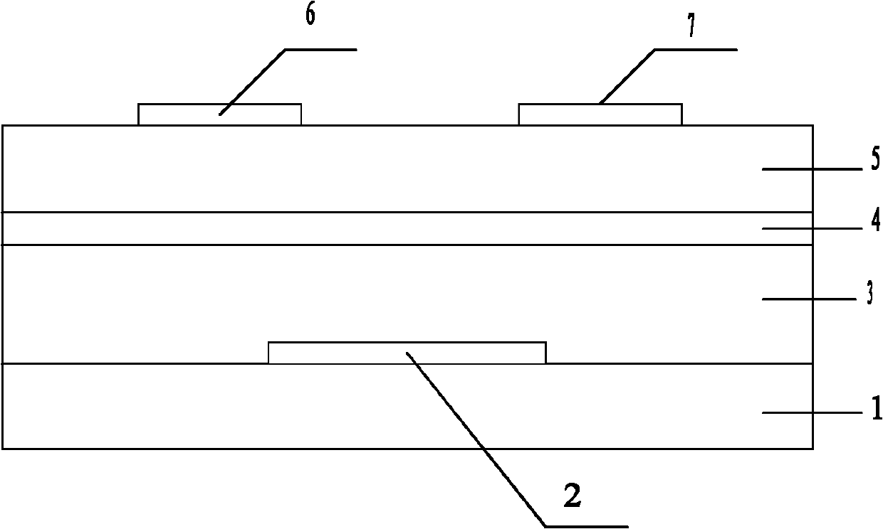

Image

  • Polymer semiconducting material and organic thin film transistor
  • Polymer semiconducting material and organic thin film transistor
  • Polymer semiconducting material and organic thin film transistor

Examples


preparation example Construction

[0083] I. Preparation of polymerized monomers

[0084] (1) Preparation of 2,5-dibromo-3,4-dialkylthiophene:

[0085] Prepared according to the method provided in the literature (Chem. Eur. J., 2004, 3331-3340), the reaction equation is as follows.

[0086] First prepare 3,4-dialkylthiophene: use 3 times the molar amount of magnesium chips, 2.8 times the molar amount of 1-bromoalkane as raw material, diethyl ether as solvent, and the concentration of the reaction system is 2 mol / liter to prepare alkyl bromide Magnesium chloride solution; under anhydrous and anaerobic conditions, add commercially available 1 times molar amount of 3,4-dibromothiophene, 3% molar amount of Ni(dppp) to another reaction flask equipped with a constant pressure dropping funnel Cl 2 and diethyl ether (the concentration of the reaction system is 0.75 mol / liter), introduce the prepared Grignard reagent into a constant pressure dropping funnel, heat to slightly boiled reaction for 12 hours after the addi...

Embodiment 1

[0110] Embodiment 1: the synthesis of N-dodecyl-2,7-dibromo-3,6-diiodocarbazole

[0111] Heat the mixture of 10mmol N-dodecyl-2,7-dibromocarbazole (4.93g) and 100ml glacial acetic acid to 80°C, the solid dissolves, and add 26.7mmol KI (4.43g) and 13.3mmolKIO in one go 3 (2.85g), after stirring at 80°C for 6 hours, pour it into water, extract with dichloromethane, wash with saturated brine, dry over anhydrous magnesium sulfate, remove the solvent, and recrystallize with acetone to obtain 5.20g of white solid, namely N-dodecyl-2,7-dibromo-3,6-diiodocarbazole, yield: 70.1%, structural characterization data are as follows: 1 H NMR (300MHz, CDCl 3 ): δ (ppm) 8.46 (s, 2H), 7.68 (s, 2H), 4.14 (t, 2H, J=7.2Hz), 1.79-1.83 (m, 2H), 1.24-1.32 (m, 18H), 0.88(t, 3H, J=6.3Hz). Elemental analysis (C 24 h 29 Br 2 I 2 N (%)): Calculated: C, 38.69; H, 3.92; N, 1.88. Measured: C, 38.50; H, 3.80; N, 1.82.

Embodiment 2

[0112] Example 2: Synthesis of N-dodecyl-2,7-dibromo-3,6-bis(trimethylsilylacetylene)carbazole

[0113] Under argon atmosphere, to compound 16.0mmol N-dodecyl-2,7-dibromo-3,6-diiodocarbazole (11.9g), 224mg bis(triphenylphosphine)palladium dichloride (Pd (PPh 3 ) 2 Cl 2 ), 60.9mg cuprous iodide (CuI), 32.7mmol trimethylsilylacetylene (3.20g) was slowly added dropwise to a mixture of 80ml tetrahydrofuran and 80ml triethylamine, stirred at room temperature for 48 hours, washed with ethyl acetate, collected organic phase, washed the organic phase twice with saturated ammonium chloride solution and saturated brine respectively, dried over anhydrous magnesium sulfate, removed the solvent, and purified by silica gel column chromatography. The eluent was 1 / 4 dichloromethane / petroleum by volume Ether, 6.18g of solid was obtained, that is, N-dodecyl-2,7-dibromo-3,6-bis(trimethylsilylacetylene)carbazole, the yield: 56.4%, and the structural characterization data are as follows: 1 H N...


PUM

PropertyMeasurementUnit
thicknessaaaaaaaaaa
thicknessaaaaaaaaaa

Abstract

The invention provides a compound with a structure shown in a formula (I) in the specification, a polymer and a polymer semiconducting material. An N atom is introduced into the compound and an alkyl chain is introduced into the N atom, so that the polymer based on the compound containing N and S hetero atoms has excellent solubility in an organic solvent. Furthermore, the compound provided by the invention contains thiofuran rings at two ends, and can effectively reduce the steric hindrance between adjacent units in the polymer based on the compound containing N and S hetero atoms, and improve the conjugation degree of the polymer, thus guaranteeing that an organic thin film transistor using the polymer semiconducting material has high mobility. The invention also provides the organic thin film transistor using the polymer semiconducting material. Experiment results show that the organic thin film transistor provided by the invention has a mobility of 0.073 cm<2> / V.s.

Description

technical field [0001] The invention relates to the technical field of semiconductor materials, more specifically, to a polymer semiconductor material and an organic thin film transistor. Background technique [0002] Polymer semiconductor material is a new type of semiconductor material that has both the optical and electrical properties of inorganic semiconductors and the convenience of artificial synthesis of polymers, and is widely used in the field of organic thin film transistors. Because polymer semiconductor materials can be prepared by solution spin coating, printing, printing and other processing methods to obtain electronic devices such as organic thin film transistors with low cost, they have attracted much attention in recent years. Regioregular poly(3-hexylthiophene) (rr-P3HT) is the first polymeric semiconductor material with excellent hole transport properties, and its mobility can reach 0.1 cm 2 / V·s (Nature, 1999, 401, 685-688.). However, due to the high ...

Claims


Application Information

Patent Timeline
Patent Type & Authority Applications(China)
IPC IPC(8): C07D495/14C08G61/12H01L51/30
Inventor 耿延候陈亚刚田洪坤
Owner CHANGCHUN INST OF APPLIED CHEMISTRY - CHINESE ACAD OF SCI
Why Eureka
Try Eureka