Copper plating substrate-based method for preparing large-area graphene film

A technology of electroplating copper and graphene, applied in sputtering plating, ion implantation plating, gaseous chemical plating, etc., can solve the problems of high growth cost, small area, fragile substrate, etc., and achieve surface flatness High, simple method, high effect

Active Publication Date: 2011-10-12
SHANGHAI INST OF MICROSYSTEM & INFORMATION TECH CHINESE ACAD OF SCI
View PDF4 Cites 35 Cited by
  • Summary
  • Abstract
  • Description
  • Claims
  • Application Information

AI Technical Summary

Problems solved by technology

However, how to prepare high-quality and large-area graphene films on a large scale is still a difficult problem. At present, the methods for growing graphene mainly include: mechanical exfoliation method, the obtained graphene is of high quality but the area is small, and the efficiency is also very low; redox method, the operation is simple and the cost is low, but graphene will cause the loss of some physical and chemical properties during the redox process, and the obtained graphene area is also small; the silicon carbide cracking method can obtain large-area graphene, but graphite The quality of graphene is greatly affected by the substrate, and the growth cost is also high, requiring a high-temperature vacuum environment; chemical vapor deposition is suitable for large-scale preparation of graphene, but it is relatively constrained by the metal substrate
[0004] At present, the metal substrates commonly used in chemical vapor deposition methods include Cu, Ni, Ru, etc. For Cu substrates, there are mainly two types of sputtered copper or copper foil on silicon wafers, but these two Cu substrates are in There are certain defects in the preparation process: the sputtered copper is easy to condense into island-shaped particles at high temperature, and the area of ​​the prepared graphene is too small; the copper foil is easy to bend and wrinkle during the operation process, which affects the quality of the substrate. Flatness
[0005] This invention intends to propose a graphene growth method based on an electroplated copper substrate, which is compatible with the IC process and has high preparation efficiency, which solves the problems of difficult patterning, fragile substrates, and small area in the previous graphene preparation process.

Method used


Image

  • Copper plating substrate-based method for preparing large-area graphene film
  • Copper plating substrate-based method for preparing large-area graphene film
  • Copper plating substrate-based method for preparing large-area graphene film

Examples


Embodiment 1

[0025] Example 1: Preparation of large-area graphene film based on electroplated copper substrate

[0026] The production process is as follows:

[0027] 1. Oxidize single crystal silicon with 200nm SiO 2 Oxide layer, and then sputter a seed layer of 50nmNi / 200nmCu on the oxide layer;

[0028] 2. Electroplate copper with a thickness of 4 μm on the seed layer of the above silicon wafer, the electroplating current is 2A, and the electroplating time is 18 minutes;

[0029] 3. Divide the silicon wafer into the size of the required substrate, load it into a quartz boat, put it into the constant temperature zone of the quartz tube, and raise the temperature to 1000°C in an atmosphere of 300 sccm argon;

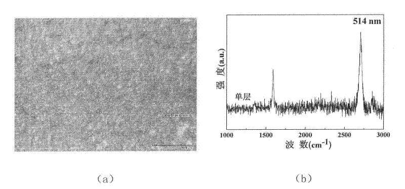
[0030] 4. When the target temperature is 1000°C, feed 10sccm methane, 200sccm hydrogen and 800sccm argon, grow for 3 minutes, and then anneal with the furnace in an atmosphere of 200sccm argon to produce a large-area graphene film. The experimental results are shown in the figure...

Embodiment 2

[0031] Embodiment 2: Prepare multilayer graphene film based on electroplated copper substrate

[0032] Steps 1, 2, and 3 are the same as Steps 1, 2, and 3 of Example 1, and the temperature is raised to 800° C.;

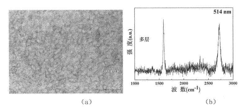
[0033] 4. When the target temperature is 800°C, feed 15sccm methane, 100sccm hydrogen and 400sccm argon, grow for 5 minutes, and then anneal in the furnace under the atmosphere of 200sccm argon to produce multilayer graphene. The experimental results are shown in the figure below: figure 2 (a) is the optical image after growth; figure 2 (b) is a Raman spectrum, and the Raman spectrum shows that graphene is multi-layered.

Embodiment 3

[0034] Example 3: Preparation of highly striped graphene film based on electroplated copper substrate

[0035] Step 1 is identical with embodiment 1 step 1;

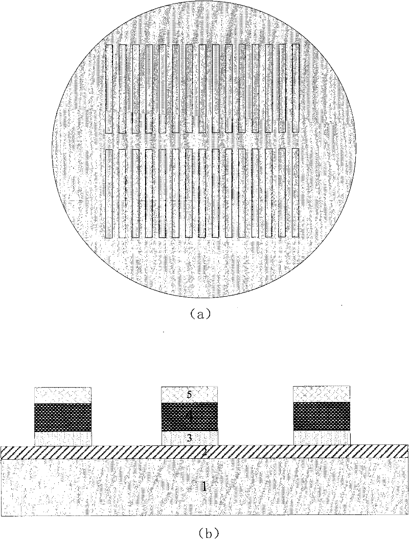
[0036] 2. Patterning of the seed layer: the photolithography version is as follows figure 1 As shown, the striped area is the area of ​​electroplated copper (2μm×10μm), after coating a 5μm thick glue, photolithography and development;

[0037] 3. Electroplating copper: electroplating current 1.8A, electroplating time 15min, electroplating copper thickness 3.5um;

[0038] 4. Remove the photoresist after electroplating, then soak in the mixed solution of dilute sulfuric acid and hydrogen peroxide for tens of seconds after cleaning, remove the seed layer Ni / Cu, and divide it into substrates of corresponding sizes according to the image after cleaning (the substrate structure is shown in the figure below 5);

[0039] Example 3: Preparation of highly striped graphene film based on electroplated copper substrate

[0040] S...


PUM

PropertyMeasurementUnit
thicknessaaaaaaaaaa
thicknessaaaaaaaaaa
thicknessaaaaaaaaaa

Abstract

The invention relates to a method for preparing graphene on a copper plating substrate. The method is characterized by comprising the following steps of: preparing the graphical copper plating substrate on a silicon chip; and growing the graphene on the copper plating substrate for 2 to 5 minutes at the temperature of between 800 and 1,000 DEG C by using a normal pressure chemical vapor deposition method, using methane as a carbon source and using argon and hydrogen as carrier gases. A graphical graphene film can be directly prepared by the method, and the substrate can be compatible with an integrated circuit (IC) process; and the manufacturing method is simple and low in cost, and can be used for large-scale manufacture.

Description

technical field [0001] The invention relates to a method capable of producing graphene films on a large scale, more specifically to a method for preparing large-area graphene films based on an electroplated copper substrate, and belongs to the field of graphene film preparation. Background technique [0002] Graphene, that is, single-layer graphite, is a substance in which carbon atoms are arranged in a honeycomb structure on a plane. It was once considered a purely theoretical material because it was believed to be unstable. However, in 2004, after Geim et al. discovered the independent graphene, some experimental work successively verified that the carriers in graphene are Dirac fermions without static mass. Since then, graphene research boom has begun. [0003] At present, graphene has been proven to have good application prospects in nanoelectronic devices, single-electron transistors, thermoelectric aspects, and conductive films. However, how to prepare high-quality an...

Claims


Application Information

Patent Timeline
Patent Type & Authority Applications(China)
IPC IPC(8): C23C16/26C23C16/04C23C28/00C23C14/16C23C14/18C25D3/00
Inventor 李铁王文荣周玉修王跃林
Owner SHANGHAI INST OF MICROSYSTEM & INFORMATION TECH CHINESE ACAD OF SCI
Why Eureka
Try Eureka