Wavelength up-conversion semiconductor structure and optical detection method thereof

A technology of semiconductors and wavelengths, which is applied in semiconductor devices, using electric radiation detectors for photometry, electrical components, etc., can solve the problems of high dark counts of detectors and the inability to obtain a high enough signal-to-noise ratio, and achieve the goal of reducing dark counts Effect

Active Publication Date: 2012-01-04
TSINGHUA UNIV
View PDF5 Cites 8 Cited by
  • Summary
  • Abstract
  • Description
  • Claims
  • Application Information

AI Technical Summary

Problems solved by technology

[0006] In order to solve the problem that a sufficiently high signal-to-noise ratio cannot be obtained due to the high dark count of the detector when detecting extremely weak infrared light, the present invention proposes a wavelength up-conversion semiconductor structure, including: a substrate, a lower electrode contact layer, and a lower transition layer , a wavelength up-conversion region, an upper transition layer, and an upper electrode contact layer, characterized in that: the wavelength up-conversion region includes at least two quantum well layers and a barrier layer between the two, and the quantum well layer- 1 and the quantum well layer-2 can be quantum wells at the same time, or one of them is a quantum dot; the energy difference between the electronic excited state energy level and the electronic ground state energy level in the quantu

Method used


Image

  • Wavelength up-conversion semiconductor structure and optical detection method thereof
  • Wavelength up-conversion semiconductor structure and optical detection method thereof
  • Wavelength up-conversion semiconductor structure and optical detection method thereof

Examples


Embodiment 1

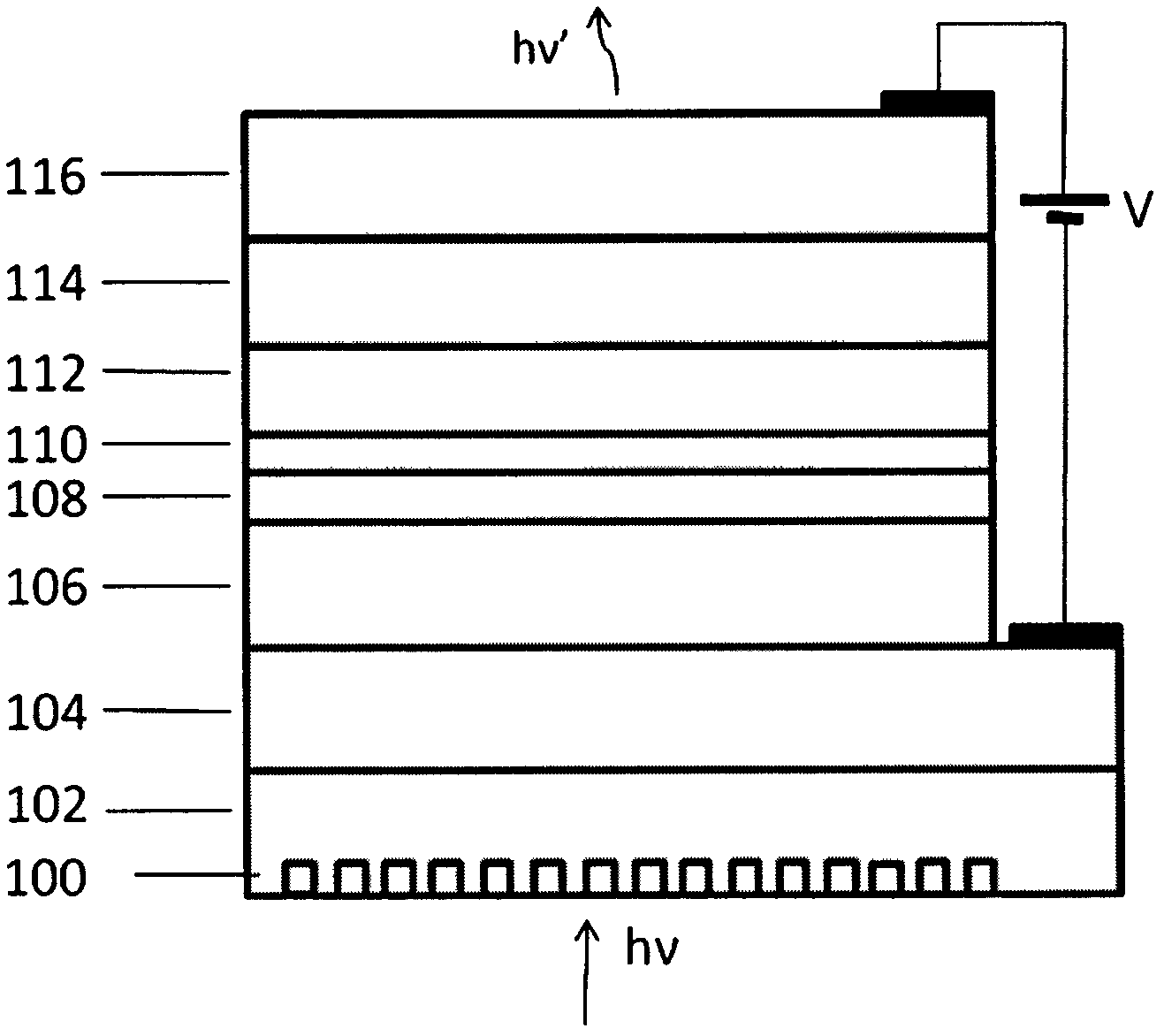
[0023] The structure of the 7μm infrared light up-conversion device described in this example is as follows figure 1 As shown, the structural material is sequentially grown on a GaAs substrate using typical semiconductor material epitaxy techniques such as molecular beam epitaxy and metal-organic chemical vapor deposition techniques. The grating structure on the GaAs substrate is made by semiconductor processing technology.

[0024] Among them, 100 is a grating structure, which is used to convert the infrared light incident on the vertical surface into components that can be absorbed by the quantum well subband, 102 is the GaAs substrate, 104 is the n-type GaAs lower electrode contact layer, and 105 is 30nm n-type Al 0.3 Ga 0.7 As transition layer, 106 is 50nm Al 0.8 Ga 0.2 As transition layer, 108 is a doping concentration of 8×10 18 cm -3 , an n-type GaAs quantum well layer with a thickness of 4nm, 110 is a 2nm AlAs barrier layer, and 112 is an 8nm Al 0.2 Ga 0.8 As qu...

Embodiment 2

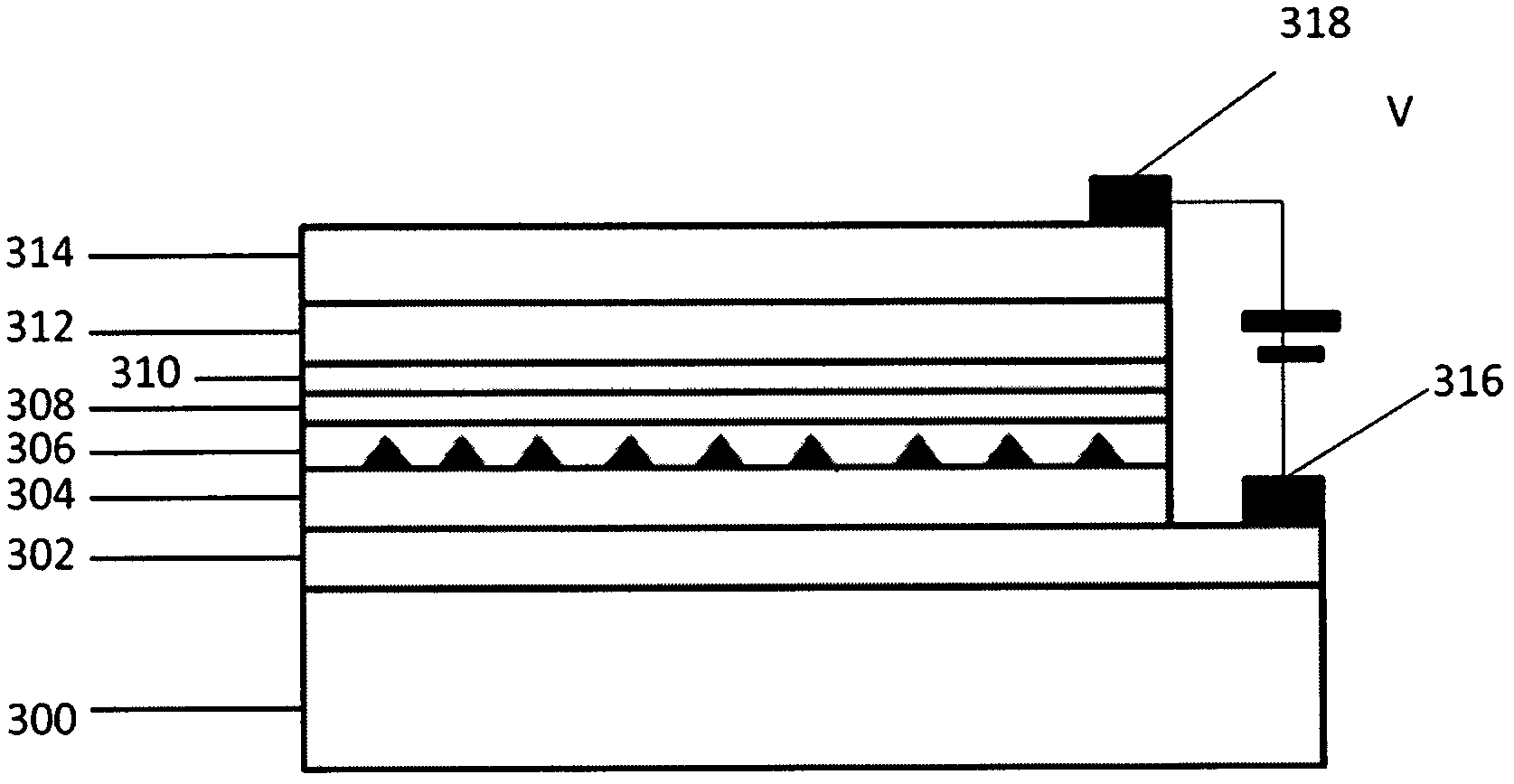
[0028] The structure of the 2μm infrared light up-conversion device described in this example is as follows image 3 As shown, the structural material is sequentially grown on a sapphire substrate using typical semiconductor material epitaxy techniques, such as molecular beam epitaxy technology, metal-organic chemical vapor deposition technology, etc.

[0029] Among them, 300 is a sapphire substrate, 302 is a 200nm n-type AlN lower electrode contact layer, 304 is a 100nm AlN transition layer, 306 is a GaN quantum dot with an average size of 4nm, 308 is a 2nm AlN barrier, and 310 is a 2nm Al 0.3 Ga 0.7 N quantum well, 312 is a 100nm AlN transition layer, 314 is a 100nm p-type GaN upper electrode contact layer, 316 is an n-type electrode, and 318 is a p-type electrode.

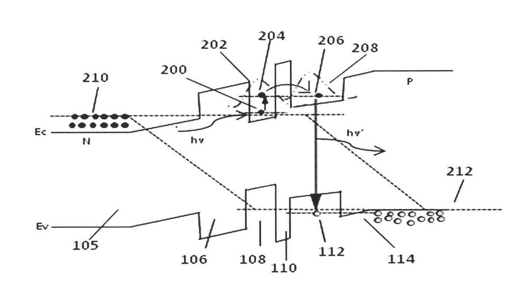
[0030] The energy band structure of the 2 μm infrared light up-conversion device described in this example is as follows Figure 4 shown. 400 is the ground state energy level of GaN quantum dot conduction ban...

Embodiment 3

[0033] The structure of the 3.1 μm infrared light up-conversion device described in this example is as follows Figure 5 As shown, the structural material is sequentially grown on a GaAs substrate using typical semiconductor material epitaxy techniques such as molecular beam epitaxy and metal-organic chemical vapor deposition techniques.

[0034] Among them, 500 is GaAs substrate; 502 is n+Al 0.5 Ga 0.5 As lower electrode contact layer, thickness 300nm; 504 is n-Al 0.5 Ga 0.5 As transition layer, thickness 500nm; 506 is i-Al 0.5 Ga 0.5 As transition layer, thickness 50nm; 508 is i-Al 0.8 Ga 0.2 As electron blocking layer, thickness 50nm; 510 is i-Al 0.5 Ga 0.5 As transition layer, thickness 50nm; 512 is i-Al 0.25 In 0.75 As quantum dots, the average size of quantum dots is 8nm, the energy difference between the conduction band ground state energy level and the excited state energy level of quantum dots is 0.4eV, and the quantum dot conduction band excited state energ...


PUM

PropertyMeasurementUnit
Thicknessaaaaaaaaaa

Abstract

The invention provides a wavelength up-conversion semiconductor structure and an optical detection method thereof, belonging to the semiconductor material and device preparation field. The wavelength up-conversion semiconductor structure is characterized in that: the wavelength up-conversion semiconductor comprises at least two quantum well layers and a barrier layer between the two layers, energy difference between an electrical excitation state energy level in a quantum well layer-1 and an electrical ground state energy level is corresponding to infrared photon energy, and energy differencebetween an electrical ground state energy level in a quantum well layer-2 and the electrical excitation state energy level in the quantum well layer-1 is less than 50meV. According to the invention, a dark count introduced in a wavelength up-conversion process can be greatly reduced. The invention provides an infrared low-light detection method based on the wavelength up-conversion semiconductor structure, and is characterized in that: when an infrared photon is absorbed, an electron at a ground state energy level in the quantum well layer-1 moves to an excitation state energy level and enters the quantum well layer-2 through resonance tunneling, and an electron cavity carries out recombination emission of a low wave length photon which can be detected by an optical detector with an extremely dark count.

Description

Technical field: [0001] The invention belongs to the field of semiconductor material and device manufacture, and in particular relates to a semiconductor device structure for infrared weak light detection. Background technique: [0002] Infrared detection technology plays a very important role in environmental pollution monitoring, meteorological detection, thermal imaging, astronomical observation and military fields. At present, the technical routes applied to weak infrared light detection mainly include: infrared detectors based on HgCdTe (MCT) semiconductor materials, infrared detectors based on narrow bandgap semiconductor InSb and its type II quantum wells, and infrared detectors based on quantum well intersubband transitions. Quantum well infrared detectors (QWIP), quantum dot infrared detectors (QDIP) based on quantum dot intersubband transitions, and infrared detectors based on wavelength upconversion. Due to the extremely low light intensity of the infrared signal...

Claims


Application Information

Patent Timeline
IPC IPC(8): H01L31/0352H01L31/101G01J1/42
Inventor 罗毅郝智彪
Owner TSINGHUA UNIV
Why Eureka
Try Eureka