Preparation method of crystalline silicon solar cell

A solar cell, crystalline silicon technology, applied in circuits, electrical components, semiconductor devices, etc., can solve the problems of the decline of the life of the minority carrier, the inability to form ohmic contacts, the warpage of difficult crystalline silicon solar cells, etc., to improve absorption, increase Back passivation effect, effect of reducing influence

Inactive Publication Date: 2012-05-02
苏元周
View PDF3 Cites 12 Cited by
  • Summary
  • Abstract
  • Description
  • Claims
  • Application Information

AI Technical Summary

Problems solved by technology

These two back passivation methods have their drawbacks: in the first method, since the bulk minority carrier lifetime in silicon wafers is highly sensitive to high-temperature processes, especially polysilicon wafers, the thermal oxidation growth process above 900 °C will cause The bulk minority carrier lifetime in silicon wafers obviously declines; the second implementation method, the stacking of silicon nitride and silicon dioxide, is difficult to solve the warpage problem of crystalline silicon solar cells
On the other hand, the insulation of the back passivation structure blocks the silicon chip and the back electrode, resulting in the inability to form an ohmic contact between the silicon chip and the back electrode

Method used


Image

  • Preparation method of crystalline silicon solar cell
  • Preparation method of crystalline silicon solar cell

Examples


Embodiment 1

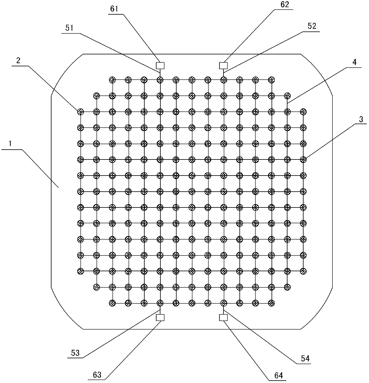
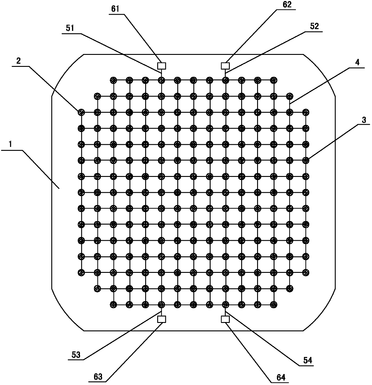
[0026] A method for preparing a crystalline silicon solar cell proposed by the present invention is divided into the following steps according to the production sequence of the process line: making texture on the silicon wafer; diffusing on the silicon wafer to make a PN junction; performing deedge junction treatment on the silicon wafer; Passivate the surface of the silicon wafer; make front and back electrodes; sinter.

[0027] In this specific embodiment, conventional processes are used for texturizing the silicon wafer, making PN junctions by diffusion on the silicon wafer, deedge-junctioning the silicon wafer, fabricating front electrodes and sintering.

[0028] In this specific example, a 13.56MHz plasma-enhanced chemical vapor deposition (PECVD, Plasma Enhanced Chemical Vapor Deposition) process is used to perform double-sided passivation treatment on both surfaces of the silicon wafer, and the specific treatment process is as follows:

[0029]1) A 13.56MHz plasma-enhan...

Embodiment 2

[0046] This embodiment is basically the same as the first embodiment, except that the process conditions used to passivate the surface of the silicon wafer are different.

[0047] In this embodiment, the specific process conditions for coating aluminum oxide film are: power is 3000W, vacuum degree is 1.8 Torr, flow rate of high-purity oxygen is 3.7 liters / minute, flow rate of trimethylaluminum is 0.42 liters / minute, substrate The temperature is 500°C, the deposition time is determined by the speed of depositing aluminum oxide film, the thickness of aluminum oxide film is 50nm; the specific process conditions of front passivation are: power is 2500W, vacuum degree is 1.7 torr, high-purity ammonia gas flow rate is 4 liters per minute, the substrate temperature is 420°C, and the passivation time is 4 minutes; the specific process conditions for plating silicon nitride films are: power 3500W, vacuum degree 1.5 Torr, high-purity ammonia flow rate 7 liters / minutes, the silane flow ...

Embodiment 3

[0049] This embodiment is basically the same as the first embodiment, except that the process conditions used to passivate the surface of the silicon wafer are different.

[0050] In this embodiment, the specific process conditions for coating the aluminum oxide film are: the power is 3000W, the vacuum degree is 1.5 Torr, the flow rate of high-purity oxygen is 4.5 liters / minute, the flow rate of trimethyl aluminum is 0.47 liters / minute, the substrate The temperature is 470°C, the deposition time is determined by the speed of depositing aluminum oxide film, the thickness of aluminum oxide film is 170nm; the specific process conditions of front passivation are: power is 2500W, vacuum degree is 1.8 torr, high-purity ammonia gas flow rate is 6 liters per minute, the substrate temperature is 480°C, and the passivation time is 3.5 minutes; the specific process conditions for plating silicon nitride films are: power 3500W, vacuum degree 1.8 Torr, high-purity ammonia flow rate 3.5 lite...


PUM

PropertyMeasurementUnit
thicknessaaaaaaaaaa
widthaaaaaaaaaa
lengthaaaaaaaaaa

Abstract

The invention discloses a preparation method of a crystalline silicon solar cell. In the passivation process technology of the back surface of a silicon wafer, because aluminum oxide has constant negative charge, the composition of the back surface can be lowered, and the same time, because silicon nitride in rich in hydrogen, passivation can be realized effectively, and in addition, the passivation overlapping layers of aluminum oxide and silicon nitride act as a back reflector, the absorption of long beam waves can be improved greatly, the passivation overlapping layers are positioned between a back surface electrode and the silicon wafer, the warping degree of the crystalline silicon solar cell can be lowered greatly, and the influence on the lifetime of a minority carrier in the silicon wafer can be lowered effectively; and when the back surface electrode is manufactured, because the passivation overlapping layers for the corrosion depth in the corrosion region is just removed, the problem that the back surface electrode and the silicon wafer have less possibility of forming favorable ohmic contact due to the back surface passivation of the silicon wafer can be solved effectively, at the same time, a dense network structure is formed by connecting all the adjacent electric conducting materials by utilizing a silver wire, and the network structure is especially favorable for the collection and conduction of back surface current carriers of the silicon wafer.

Description

technical field [0001] The invention relates to a manufacturing process of a solar cell, in particular to a preparation method of a crystalline silicon solar cell. Background technique [0002] With the increasing shortage of conventional energy sources, renewable energy has been paid more and more attention by human beings. In the past ten years, the amount of solar power generation has shown an exponential growth. With the continuous improvement of the manufacturing process of solar cells and the continuous reduction of production costs, Solar cells will become more and more popular. [0003] At present, the manufacturing process of solar cells has been standardized. According to the production sequence of the process line, it is divided into the following steps: 1. Texturing the silicon wafer: through chemical reactions, the original bright silicon wafer surface (including the front and back) is formed into uneven texture. structure to extend the propagation path of lig...

Claims


Application Information

Patent Timeline
Patent Type & Authority Applications(China)
IPC IPC(8): H01L31/18H01L31/0216H01L31/0224
CPCY02P70/50
Inventor 蒋旭东黄志林肖剑峰
Owner 苏元周
Why Eureka
Try Eureka