

Microwave device ceramic substrate material and preparation method thereof
A ceramic substrate and microwave device technology, which is applied in the field of microwave device ceramic substrate materials and its preparation, can solve problems such as machinability, etc., and achieve a ceramic particle structure that is dense and can be finely processed, with a high Q value and a good dielectric constant. Effect
- Summary
- Abstract
- Description
- Claims
- Application Information
AI Technical Summary
Problems solved by technology
Method used
Image

Examples
Embodiment 1-7
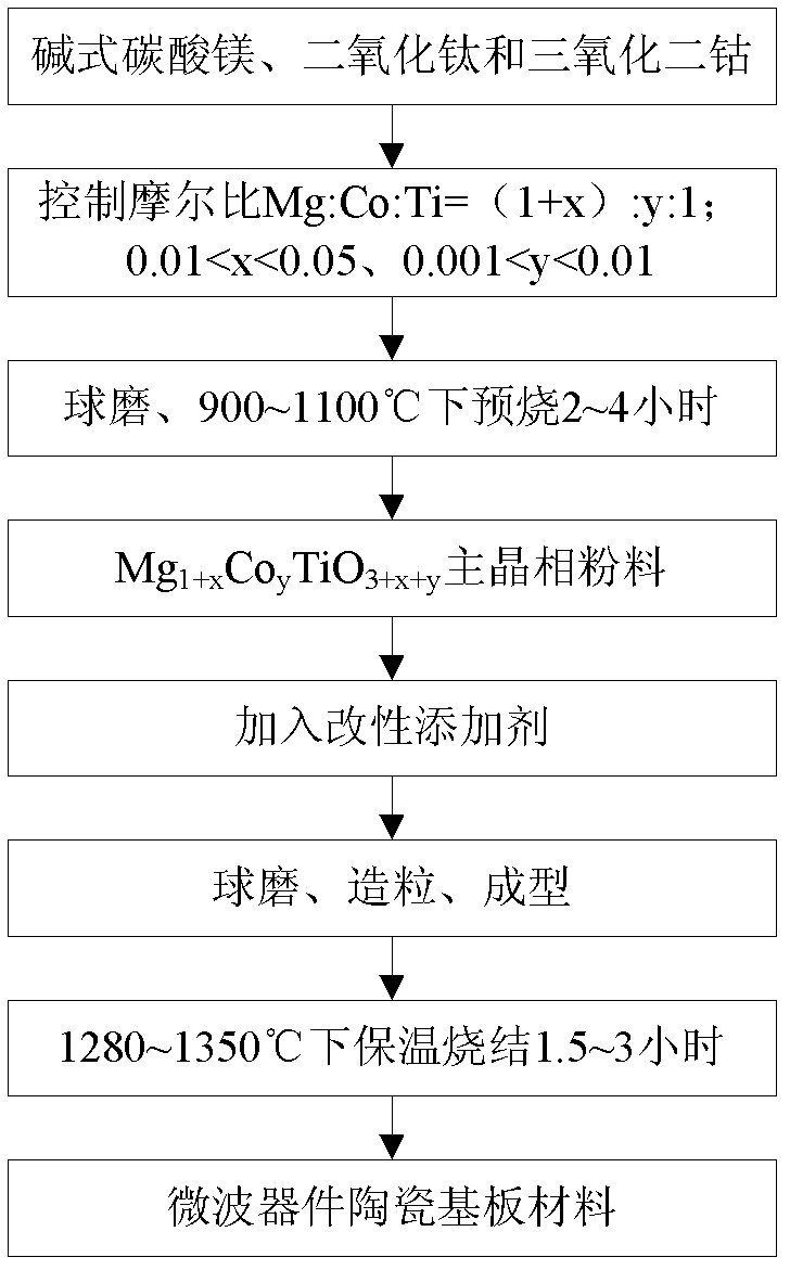
[0033] first step:
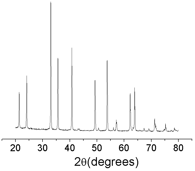
[0034] Accurately weigh the raw materials of the starting material according to the proportions in Table 1, ball mill in deionized water for 6 hours, dry, and then heat at 900-1100°C for 2-4 hours to synthesize Mg 1+x co y TiO 3+x+y .
[0035] Step two:
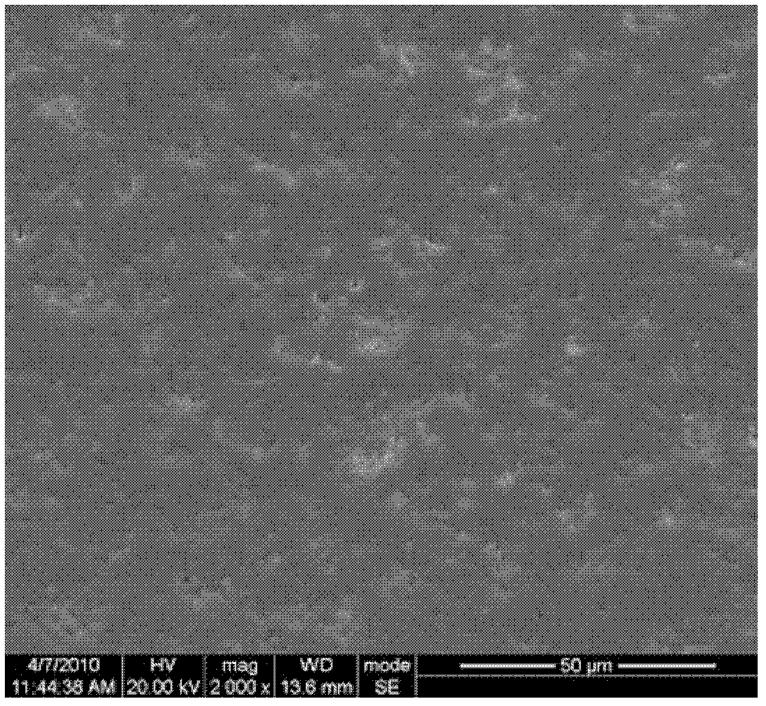
[0036] Weigh the pre-burned Mg 1+x co y TiO 3+x+y Powder 100g, wet grinding for 4 to 24 hours. Add polyvinyl alcohol aqueous solution to the dried material for granulation, dry press molding under 25MPa pressure, and sinter the green body at 1310-1350°C for 2-3 hours to obtain ceramic substrate materials for microwave devices. The sintering process and properties The test results are shown in Table 2.
[0037] Table 1 Microwave device ceramic substrate material Mg 1+x co y TiO 3+x+y Composition and pre-firing process
[0038]
[0039] Table 2 Microwave device ceramic substrate material Mg 1+x co y TiO 3+x+y process and performance
[0040]
Embodiment 8-18
[0042] Step 1: Mg 1+x co y TiO 3+x+y Synthesis: take 55.62g of basic magnesium titanate, 44.23g of titanium dioxide, and 0.15g of dicobalt trioxide, ball mill in deionized water for 6 hours, dry, and then synthesize Mg at 1000°C for 2 hours. 1.034 co 0.003 TiO 3.037 .
[0043] Step 2: Accurately weigh each raw material according to the ratio in Table 3, and wet grind for 12 hours. Add polyvinyl alcohol aqueous solution to the dried material for granulation, dry press molding under 25MPa pressure, and sinter the green body at 1280-1350°C for 1.5-3 hours to obtain microwave dielectric ceramics. The sintering process and performance test results See Table 4.
[0044] Table 3 Ceramic Substrate Materials for Microwave Devices
[0045]
[0046] Table 4 Ceramic Substrate Materials for Microwave Devices
[0047]
[0048]
PUM
 Abstract
Description
Claims
Application Information